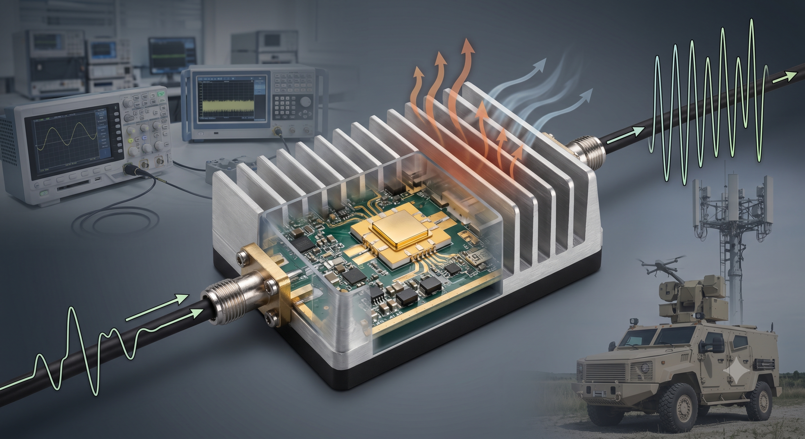
An RF Amplifier is an active electronic device designed to increase the amplitude, voltage, or overall power of high-frequency electromagnetic signals within the radio frequency spectrum. Imagine trying to transmit crucial tracking data over a vast distance, only for your signal to degrade entirely before reaching its target destination. This signal loss creates a devastating operational bottleneck where critical communication packets drop, automated UAV defensive systems fail to respond, and laboratory testing equipment yields inaccurate readings. To solve this degradation, B2B system engineers integrate robust active amplification stages that restore signal energy, ensuring long-range reliability across even the most demanding high-frequency fields.
Turn this RF amplifier shortlist into an RFQ
If your communication system needs a validated amplifier path, CorelixRF can help translate bandwidth, output power, gain flatness, linearity, cooling and interface requirements into a practical platform recommendation.
How Do RF Amplifiers Boost Low-Power Signals?
An active RF Amplifier boosts low-power signals by drawing external direct current (DC) power and converting it into high-frequency alternating current (AC) signal energy. This conversion process relies on active semiconductor components that scale up weak incoming voltages while maintaining signal integrity across the signal chain. If your system is starved of this vital energy conversion, long-distance cables will quickly attenuate your transmissions.
What Is the Active Transistor Conversion Process?
Active transistors utilize a controlled DC bias network to regulate the physical transition of electrical energy. Think about it: without a constant, stable DC bias, your weak input signals cannot modulate the larger current paths required for B2B transmissions.

To keep the signal clean, modern test systems must match impedances carefully. You can observe this exact layout on a high-precision testing bench where performance is constantly validated.
- DC Coupling Networks: These prevent unwanted power reflections inside the circuit.
- Input Matching: This optimizes signal reception parameters.
- Output Stages: These drive high current into the load.
How Does Power Gain Affect System Budgets?
Power gain is measured by comparing the energy entering the input port to the amplified signal exiting the output. Understanding this gain relationship helps you calculate total path losses and select the correct output stages for your remote installations.
Here is the kicker: even minor gain imbalances can cause severe downstream clipping or receiver desensitization. Key Takeaway: By planning your active amplification stages precisely, you ensure your B2B equipment delivers consistent power without overdriving sensitive receiver components.
| Parameter | Primary Unit | Operational Role | B2B Engineering Impact |
|---|---|---|---|
| Gain | Decibels (dB) | Determines amplification ratio | Scales signal levels for link budgets |
| Input Power | dBm / Watts | Sets baseline signal strength | Defines the threshold for active clipping |
| Output Power | dBm / Watts | Drives signal into the antenna | Controls maximum transmission range |
Analyzing this comparison reveals that careful balance between input thresholds and active gain is critical to avoiding receiver saturation.
Why Is Logarithmic Scaling Used for Signal Gain?
Logarithmic scaling is used for signal gain because it compresses the vast linear range of high-frequency power values into manageable mathematical additions and subtractions. When you integrate a multi-stage RF Amplifier into a complex network, cascading the system gain becomes a simple exercise in basic arithmetic rather than complex multiplication. This logarithmic approach saves B2B system architects from calculating values that range from microwatts to hundreds of kilowatts.
How Does a 3 dB Change Modify Physical Power?
A 3 dB change in signal level represents a doubling or halving of the physical power output. Want to know the best part?
- +3 dB Change: This exactly doubles your transmission power.
- +10 dB Change: This multiplies the power output by ten.
- +20 dB Change: This multiplies the power output by a factor of one hundred.
This relationship shows you why even minor calibration errors can cut your B2B transmission range in half instantly.
How Do B2B Engineers Budget Cascaded Gain?
System designers budget cascaded gain to maintain clear signal-to-noise ratios across the entire receiver chain. This mathematical budgeting ensures that your front-end components do not saturate while attempting to pull weak signals from the noise floor.
But that is not all: managing this budget prevents catastrophic damage to your downstream components. Key Takeaway: Mastering logarithmic gain budgets enables you to select the precise active stages required to maintain clear communications without wasting system power.
| Logarithmic Value (dB) | Linear Multiplication Ratio | Absolute Power Impact | Practical Application |
|---|---|---|---|
| 3 dB | 2.0x | Power is exactly doubled | Standard threshold for margin calculations |
| 10 dB | 10.0x | Power is multiplied by 10 | High-gain boosting for medium-range links |
| 20 dB | 100.0x | Power is multiplied by 100 | Severe power boosting requiring solid-state design |
Analyzing this comparison reveals that small logarithmic shifts carry massive linear power consequences that you must account for in every system design.
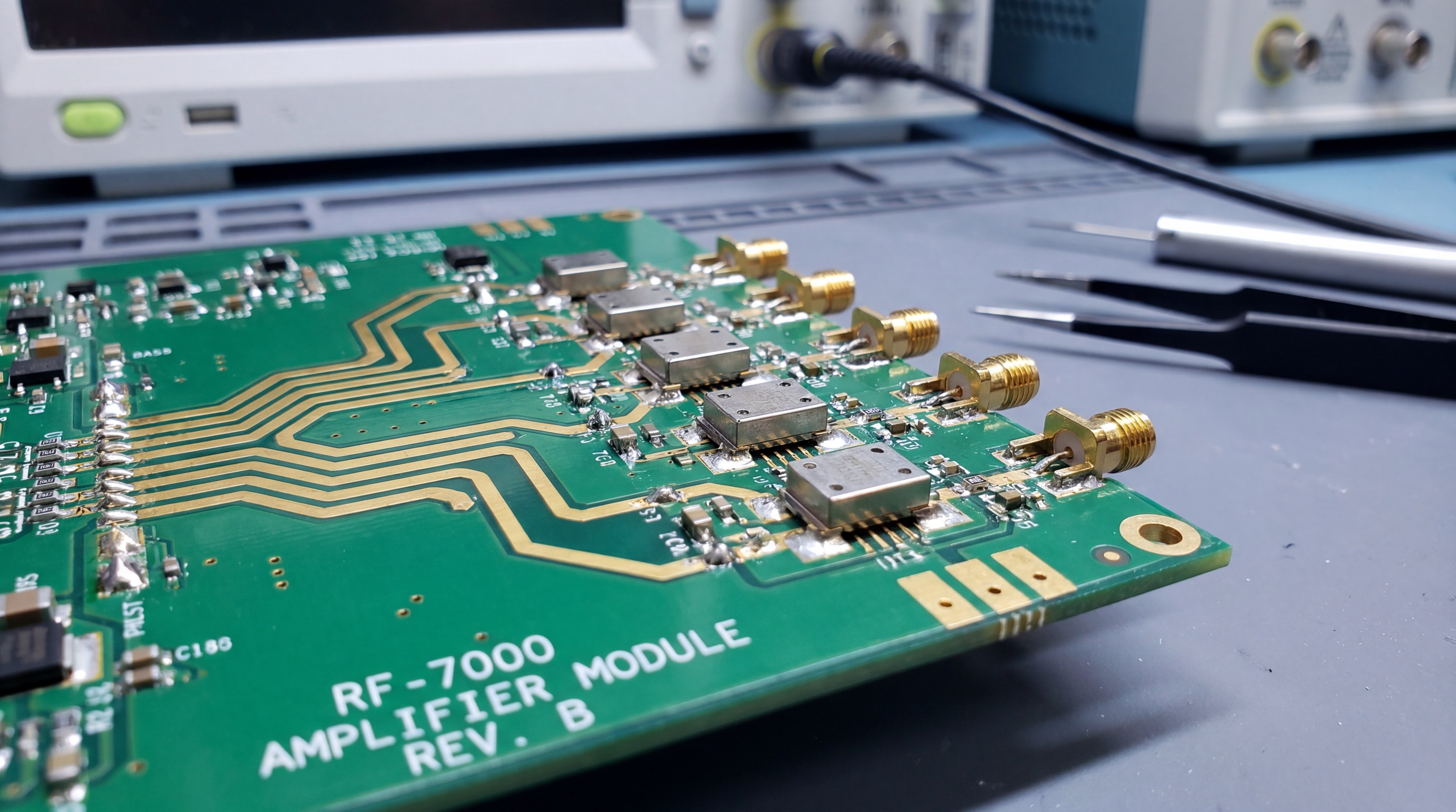
What Core Architectures Define RF Power Amps?
The core architectures that define RF power amplifiers are categorized into distinct operational classes based on their conduction angle and overall power efficiency. Selecting the correct class for your RF Amplifier determines whether your B2B design prioritizes pristine signal linearity or maximum power conversion. These architectural decisions dictate the physical footprint and thermal requirements of your final product.
How Do Linear Classes Balance Distortion?
Linear operating classes, including Class A, Class B, and Class AB, maintain signal purity by conducting current through a significant portion of the RF cycle. If you are designing for complex modulated waveforms like QAM, using standard platform platforms running in Class AB is often the ideal compromise.
Here is the kicker: Class A offers the highest linearity but wastes up to 50% of its energy as heat.
- Class A: Conducts through a full 360-degree cycle for maximum purity.
- Class B: Conducts through 180 degrees to improve power efficiency.
- Class AB: Conducts between 180 and 360 degrees to eliminate crossover distortion.
Why Are Switching Classes Used for High Power?
Switching classes like Class C, D, and E maximize efficiency by operating the active transistors as pure binary switches. This rapid switching minimizes the time the transistor spends in its active region, thereby slashing thermal power losses.
Think about it: when you need to transmit extreme power across wide ranges, prioritizing switching efficiency keeps your system running cool. Key Takeaway: Choosing the right operational class allows you to balance signal distortion against battery consumption, ensuring your field units remain active and operational.
| Amplifier Class | Conduction Angle | Theoretical Efficiency | Primary Performance Attribute |
|---|---|---|---|
| Class A | 360° | 25% to 50% | Maximum signal linearity with zero distortion |
| Class B | 180° | Up to 78.5% | Good efficiency with high crossover distortion |
| Class AB | 180° to 360° | 50% to 70% | Optimal B2B compromise for cellular signals |
| Class C | < 180° | Up to 85% | Extreme power efficiency for constant envelopes |
Analyzing this comparison reveals that as conduction angle decreases, the theoretical efficiency rises at the cost of increased harmonic distortion.
How Do Low Noise Amplifiers Protect Weak Signals?
Low noise amplifiers protect weak signals by boosting incoming electromagnetic energy while minimizing the amount of thermal noise added to the signal path. Placing this sensitive RF Amplifier stage at the absolute front-end of your receiver chain determines the ultimate range and clarity of your entire communication system. If your receiver LNA introduces excessive noise, even the most powerful transmitter will struggle to establish a reliable connection.
Why Is Noise Figure the Critical LNA Metric?
Noise figure measures the degradation of the signal-to-noise ratio as the signal passes through the active amplification stage. If you are deploying high-sensitivity receivers, integrating a broadband UHF amplifier is vital to capture weak signals before they fade entirely.
But that is not all: keeping the noise figure below 1.5 dB requires premium solid-state packaging and precise impedance matching.
- Low Noise Figure: Prevents raw signals from dissolving into background thermal hiss.
- High Input Return Loss: Keeps reflected power from corrupting delicate sensor gates.
- Stable Input Protection: Safeguards the LNA from high-power transmitter spikes.
Can LNAs and Power Amps Work Together?
Receiver front-ends integrate both LNAs and high-power transmitters into a single bi-directional system. You must isolate these components using fast-acting PIN diode switches or duplexers to prevent the transmitter from physically destroying the sensitive LNA.
Want to know the best part? This isolation allows you to use a single antenna array for both high-power output and high-sensitivity reception. Key Takeaway: Isolating your LNA and PA stages properly protects your B2B systems from self-destruction while maximizing receiver sensitivity.
| Parameter | Low Noise Amplifier (LNA) | Power Amplifier (PA) | Impact of Design Error |
|---|---|---|---|
| Primary Goal | Minimize Noise Figure (NF) | Maximize Output Power ($P_{out}$) | Poor receiver range or blown active stages |
| Typical Gain | 10 to 20 dB | 30 to 50+ dB | Weak uplink or severe downstream clipping |
| Power Handling | Microwatts to Milliwatts | Watts to Kilowatts | Thermal damage to LNA if isolation fails |
Analyzing this comparison reveals that these two active stages require completely inverted design priorities to protect signal health.
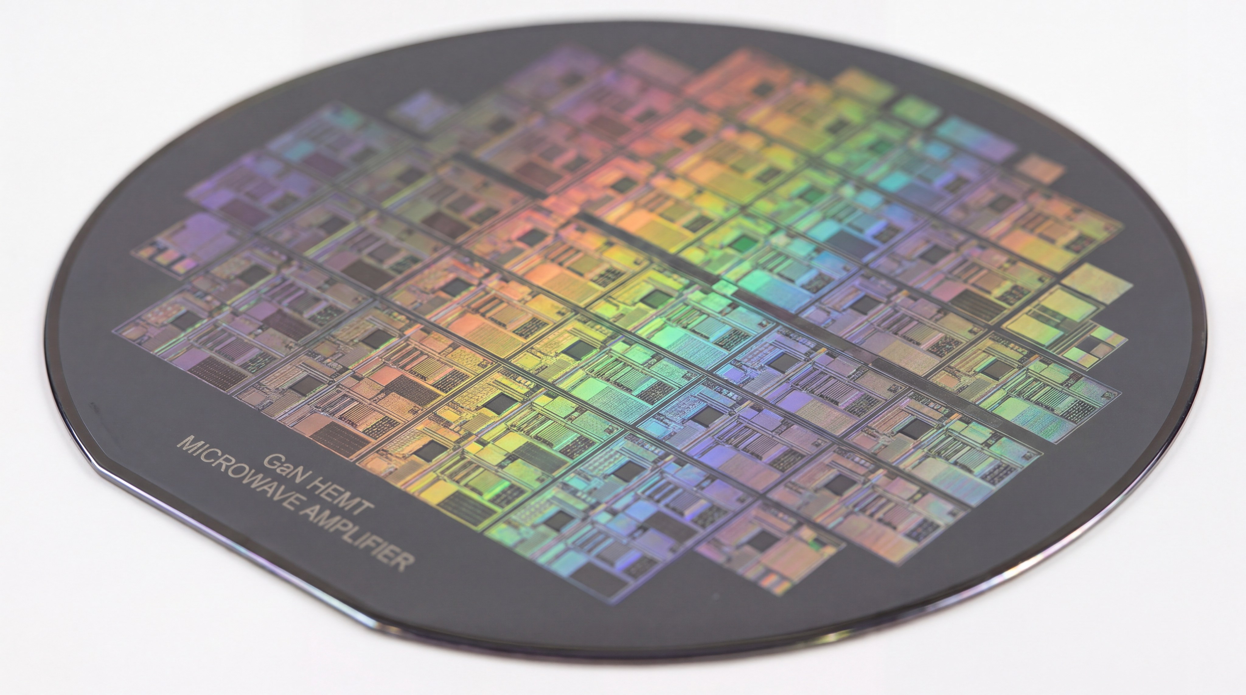
Why Are GaN Semiconductors Changing the Industry?
Gallium Nitride (GaN) semiconductors are changing the industry by providing vastly superior breakdown voltages, power densities, and thermal conductivities compared to legacy silicon or gallium arsenide. Upgrading your high-frequency system with a GaN-based RF Amplifier allows you to shrink the overall physical footprint of your equipment while generating massive output power. These wide-bandgap properties allow B2B defense and telecom systems to operate reliably at extreme voltages.
What Makes Wide Bandgap Materials Superior?
Wide bandgap materials require much higher energy levels to conduct electricity, allowing them to withstand extreme electric fields without structural breakdown. Integrating these components into your high-frequency capability platforms ensures that your systems can sweep wide bands without experiencing power drops.
Think about it: legacy materials simply melt under the high current densities that GaN processes with ease daily.
- High Breakdown Voltage: Enables safe operation at elevated system voltages.
- Superior Electron Mobility: Supports signal amplification deep into millimeter-wave bands.
- Rugged Physical Structures: Resist degradation under harsh environmental conditions.
How Does Solid-State Uptime Compare to Tubes?
Solid-state GaN platforms are rapidly replacing legacy traveling wave tube amplifiers (TWTAs) across tactical defense fields. This transition eliminates the high failure rates associated with vacuum tube filaments, significantly boosting operational lifetime.
Here is the kicker: GaN provides a graceful degradation model where single-transistor issues do not cause complete system failure. Key Takeaway: Adopting GaN solid-state architectures minimizes your B2B maintenance costs and ensures continuous uptime in critical communications.
| Semiconductor Material | Bandgap (eV) | Breakdown Field (MV/cm) | Relative Power Density | Best B2B Application |
|---|---|---|---|---|
| Silicon (Si) | 1.1 | 0.3 | Low | Low-cost consumer electronics |
| Gallium Arsenide (GaAs) | 1.4 | 0.4 | Medium | Low-noise receiver circuits |
| Gallium Nitride (GaN) | 3.4 | 3.3 | Extremely High | High-power broadband platforms |
Analyzing this comparison reveals that GaN’s wide bandgap unlocks unparalleled power density and thermal robustness for demanding environments.
What Triggers Signal Distortion and Non-Linearity?
Signal distortion and non-linearity are triggered when an active transistor is driven close to its saturation limit, causing the output signal to compress and generate unwanted harmonic frequencies. If you push your active RF Amplifier past its linear region, the system will clip the peak voltages of your modulated waveforms. This clipping creates spectral regrowth that bleeds into adjacent frequency channels, violating regulatory emission standards.
What Is the 1 dB Compression Point?
The 1 dB compression point ($P1dB$) defines the boundary where actual gain drops exactly 1 dB below the theoretical linear gain. Managing this parameter is critical when integrating custom RF front-end platforms into dynamic communication systems.
But that is not all: once an amplifier enters saturation ($Psat$), increasing the input power only worsens signal distortion without providing any extra usable output.
- Linear Region: Output power tracks input power in a perfect 1:1 ratio.
- Compression Region: Gain begins to drop as DC power limits are reached.
- Saturation Region: Output power plateaus entirely, resulting in heavy harmonic distortion.
How Do Intermodulation Products Damage Data?
Intermodulation distortion occurs when multiple input frequencies mix within a non-linear active stage, generating spurious tones. These unwanted third-order intermodulation products (IM3) are particularly dangerous because they fall directly within your operating band and cannot be filtered out.
Want to know the best part? Operating your system below its third-order intercept point (IP3) guarantees clean, interference-free transmission. Key Takeaway: Staying safely within the linear boundaries of your active stages protects your data from corruption and keeps you compliant with spectral regulations.
| Metric | Definition | Engineering Importance | Operational Impact on System |
|---|---|---|---|
| $P1dB$ | 1 dB Compression Point | Defines upper limit of safe linear operation | Standard reference for power budget design |
| $Psat$ | Saturated Output Power | Absolute maximum power capability | Causes heavy clipping; used for constant envelopes |
| $OIP3$ | Output Third-Order Intercept | Quantifies system immunity to intermodulation | High $OIP3$ ensures clean multi-carrier links |
Analyzing this comparison reveals that operating well below compression points is mandatory for maintaining signal integrity in multi-carrier B2B networks.
How Do System Integrators Manage Thermal Loads?
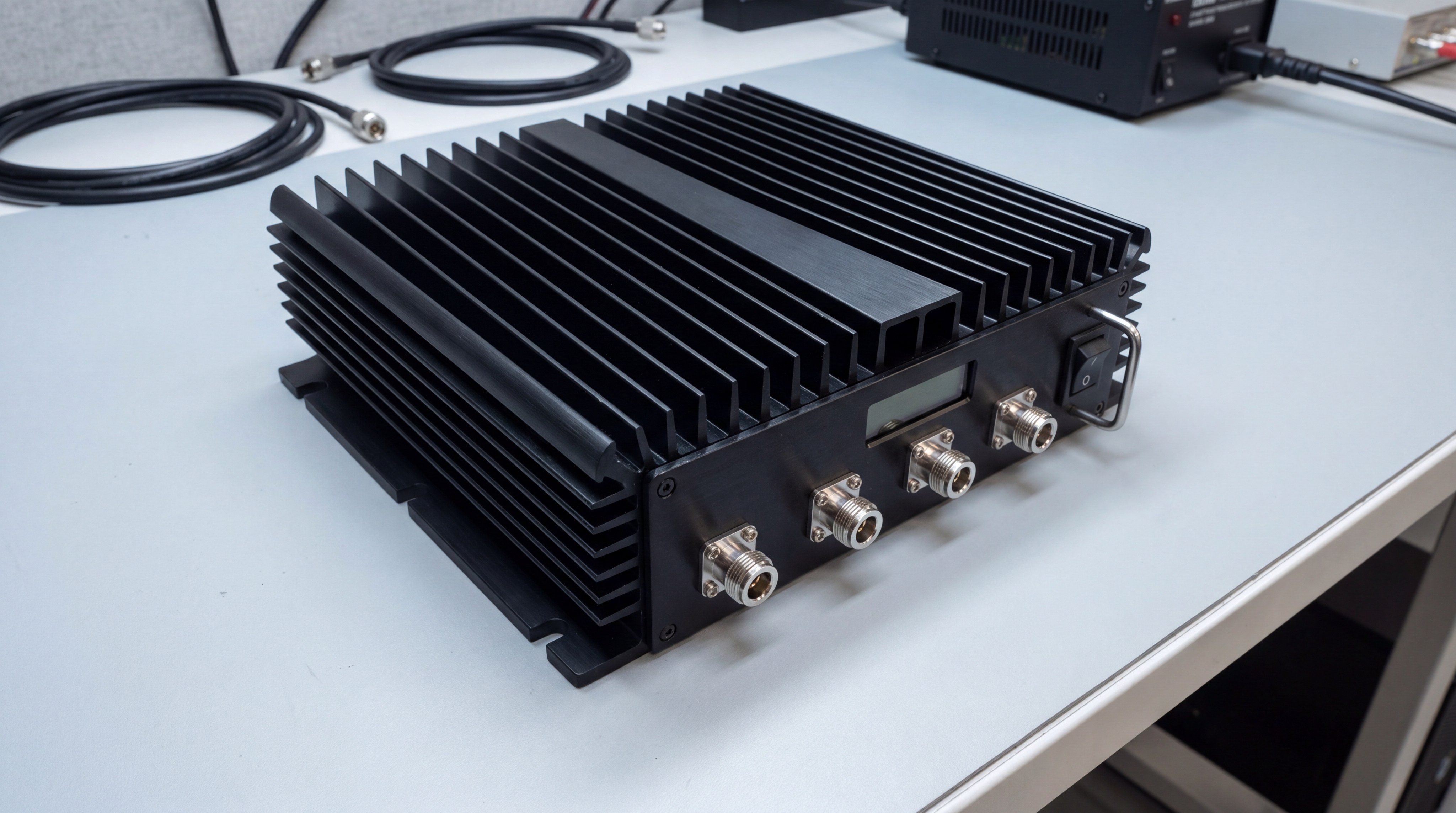
System integrators manage thermal loads by utilizing metal-backed printed circuit boards, high-conductivity heat sinks, and forced-air or liquid cooling systems to quickly draw waste heat away from the active transistor junctions. Because high-power solid-state systems convert a large percentage of DC energy directly into thermal waste, managing this heat is vital to prevent thermal runaway. A hot RF Amplifier will suffer from gain roll-off, reduced power efficiency, and a significantly shortened operating lifetime.
Which Cooling Topology Fits Your System?
Choosing between passive, forced-air, and liquid cooling depends entirely on your system’s output power and operating environment. When deploying a premium high-frequency amplifier in an enclosed rack, forced-air fans are typically required to maintain safe temperatures.
Think about it: passive heat sinks are completely silent but cannot handle the massive thermal waste generated by high-power transmitter arrays.
- Passive Cooling: Relies on natural convection; best for low-power remote poles.
- Forced-Air Cooling: Uses integrated fans to sweep heat away; standard for lab benches.
- Liquid Cooling: Uses closed-loop cold plates; required for high-kilowatt defense systems.
How Does Thermal Packaging Prevent Failures?
Thermal packaging protects your active transistors by establishing low-resistance conduction paths to the external chassis. Copper coin inserts embedded within the PCB pull heat directly from the transistor die to the massive aluminum heatsink below.
Here is the kicker: a decrease of just 10 degrees in junction temperature can double the lifespan of your active components. Key Takeaway: Prioritizing solid thermal design ensures your high-power installations survive harsh summer environments without experiencing sudden field failures.
| Cooling Method | Typical Power Target | Mechanical Complexity | Best B2B Application |
|---|---|---|---|
| Passive Heatsink | Low (< 20 Watts) | Zero complexity | Silent laboratory setups and remote installations |
| Forced Air (Fans) | Medium (20 to 500W) | Moderate complexity | Standard rack-mount systems and lab benches |
| Liquid Cold Plate | High (> 500 Watts) | High complexity | High-power military radar and jamming arrays |
Analyzing this comparison reveals that selecting a cooling method is a direct trade-off between thermal capacity and physical system complexity.
Where Are Modern RF Amplifiers Deployed Today?
Modern RF amplifiers are deployed today across tactical military counter-drone systems, national wireless telecommunications infrastructure, and high-precision laboratory test and measurement facilities. Integrating a rugged RF Amplifier into these systems ensures that electromagnetic signals can bypass background interference and reach their target receivers. Without these active boosting stages, high-speed cellular networks and tactical defensive shields would be physically unable to operate.
Why Is High Power Critical for Counter-Drone Defenses?
Counter-drone systems require high output power across broad frequency ranges to successfully block rogue UAV GPS and control links. If you are configuring these defense arrays, utilizing broadband solid-state systems is vital to establish reliable protective boundaries.
But that is not all: tactical portable systems require compact, high-efficiency gain blocks to operate on standard vehicle battery power.
- Broadband Coverage: Sweeps multiple frequency bands to neutralize agile drone frequencies.
- High Output Power: Overpowers weak control links from miles away.
- Rugged Enclosures: Protect active stages from extreme wind, rain, and heat.
How Do Labs Validate Wireless Equipment?
Laboratory testing facilities rely on ultra-flat power amplification to calibrate sensitive consumer electronics and defense systems. You must use highly linear gain blocks to ensure that your measurement equipment does not inject its own distortion into the device under test.
Want to know the best part? Flat gain allows your engineers to sweep wide frequencies without constantly recalibrating their signal sources. Key Takeaway: Selecting rugged, field-proven amplification platforms ensures your tactical or testing applications operate with absolute precision and zero down-time.
| Application Sector | Key Amplifier Requirement | Target Frequency Band | System Constraint |
|---|---|---|---|
| Counter-UAV Defense | Extreme Output Power | 400 MHz to 6 GHz | Must withstand harsh field weather |
| 5G Infrastructure | Excellent Linearity ($OIP3$) | Sub-6 GHz / Millimeter-Wave | Strict adjacent-channel leakage limits |
| Lab Testing (EMC) | Ultra-Flat Broadband Gain | 10 kHz to 40 GHz | Must tolerate high mismatched VSWR |
Analyzing this comparison reveals that different operating sectors require highly specialized, application-specific amplification parameters.
How Do Filters Prevent Interference and Added Noise?
Filters prevent interference and added noise by restricting the frequency window allowed to enter the active amplifier input or exit the output port. Because an active RF Amplifier will naturally boost every signal within its operating band, out-of-band noise must be aggressively suppressed before it saturates your sensitive receiver stages. Failing to filter these signals results in amplified background hiss that quickly drowns out your target data.
What Is the Role of Pre-Selection Filters?
Pre-selection filters block strong out-of-band signals before they can reach your sensitive input transistors. If you are operating near powerful commercial transmitters, using these bandpass filters prevents your receiver from entering premature saturation.
Here is the kicker: filtering out this noise at the input stage is the most cost-effective way to preserve your overall system dynamic range.
- Pre-Filters: Restrict the incoming spectrum to protect sensitive LNA inputs.
- Bandpass Filters: Narrow the amplified window to isolate critical signal bands.
- Harmonic Filters: Suppress spurious output frequencies from high-power switching stages.
How Is the Total Noise Figure Calculated?
The total noise figure of a cascaded signal chain is heavily dictated by the gain and noise performance of the very first active stage. Think about it: a high-gain first stage reduces the noise contribution of all subsequent downstream components, making your initial LNA choice critical. Key Takeaway: Integrating high-quality filters in tandem with your active gain stages ensures your receiver chain maintains maximum sensitivity and clear signal paths.
| Component Role | Placement Location | Primary System Function | Direct Operational Impact |
|---|---|---|---|
| Pre-Filter | Active Stage Input | Suppresses out-of-band noise | Prevents receiver saturation |
| Gain Block | Signal Chain Core | Boosts signal amplitude | Pulls weak signals from noise floor |
| Post-Filter | System Output Port | Blocks generated harmonics | Guarantees compliance with standards |
Analyzing this comparison reveals that active amplification and passive filtering are complementary technologies required to maintain overall spectral hygiene.
What Criteria Determine the Right System Selection?
The criteria that determine the right system selection include operating frequency bandwidth, output power capacity, and the specific impedance matching requirements of your target antenna. When evaluating a new RF Amplifier for your B2B application, you must balance these electrical parameters against your physical thermal dissipation limits and input voltage options. Choosing a system that is mismatched with your operating parameters will result in poor power transfer, signal distortion, or active component failure.
Why Is VSWR Tolerance Critical in the Field?
Voltage Standing Wave Ratio (VSWR) tolerance measures the system’s ability to withstand reflected signal power caused by mismatched antennas or broken cables. If your system antenna is damaged, a high-tolerance active stage will survive the resulting power reflections without burning out its output transistors.
But that is not all: maintaining a flat gain response across your entire frequency sweep is equally vital to prevent power drops during operation.
- VSWR Protection: Isolates output stages from reflected power damage.
- Gain Flatness: Guarantees flat power output across the entire sweeping bandwidth.
- Voltage Compatibility: Ensures seamless integration with standard battery or bench supplies.
How Do Environmental Limits Impact Field Use?
Extreme environmental limits, such as freezing winters or scorching summers, directly affect the performance and reliability of solid-state active devices. You must select IP-rated enclosures and ruggedized thermal systems when deploying high-frequency systems in outdoor environments.
Want to know the best part? Selecting ruggedized packaging upfront eliminates the need for expensive climate-controlled enclosures in the field. Key Takeaway: Matching your amplifier specs directly to your environmental and electrical realities guarantees a long-lasting, high-reliability deployment.
| Specification Parameter | Target Engineering Value | Primary Performance Metric | Key B2B Operational Benefit |
|---|---|---|---|
| Frequency Range | 30 MHz to 6 GHz | System Bandwidth | Wide-band operational flexibility |
| Gain Flatness | +/- 1.0 dB to +/- 2.0 dB | Power output consistency | Prevents transmission power drops |
| VSWR Rating | 2.0:1 or better | Impedance mismatch tolerance | Protects hardware from power reflections |
Analyzing this comparison reveals that selecting a system with rugged electrical and physical margins is critical to ensuring long-term field survivability.
FAQ Section
Can I run a broadband RF power amplifier directly into an antenna without any output filter?
No, you should not. Active devices naturally generate high-frequency harmonics and spurious emissions. Running an amplifier without an output filter will transmit these illegal signals directly into the air, violating strict FCC/ETSI emission limits and risking severe interference with adjacent communication bands.
What’s the best way to determine if my amplifier is driving too close to its saturation limit?
The best way is to monitor the input-to-output power ratio using a spectrum analyzer. Increase your input power in 1 dB steps; if your output power increases by less than 1 dB, your device has entered its compression region. You should back off the input power to restore a clean, linear 1:1 gain relationship.
How do I know if my solid-state amplifier’s thermal system is failing in the field?
It depends on your system’s telemetry, but the most common indicators are a sudden drop in output gain or a sharp rise in drawn current. Most modern industrial devices feature integrated thermal sensors connected to analog monitoring lines. If your chassis temperature exceeds $+85^\circ\text{C}$, the system is approaching thermal runaway and should be powered down immediately.
Can I cascade two high-gain amplifiers together to achieve a total gain of 60 dB?
Yes, you can, but you must plan the power levels carefully. The output power of your first stage plus the gain of your second stage must never exceed the second stage’s maximum input limit or compression point ($P1dB$). Additionally, cascading high-gain stages increases the risk of feedback loops, which requires inserting high-isolation attenuators between the components.
What’s the best semiconductor technology for a lightweight, battery-powered tactical jammer?
Gallium Nitride (GaN) is the undisputed gold standard for these applications. GaN offers the highest power-to-weight ratio and power efficiency of any modern solid-state technology. This extreme efficiency allows you to generate massive output power with a significantly smaller heatsink and lower power draw, maximizing your field battery life.
Conclusion
Overcoming high-frequency signal degradation, thermal waste, and non-linear distortion requires active solid-state architectures designed to withstand extreme environments. This guide has detailed how active gain mechanics, semiconductor materials like GaN, and strategic filtering protect your signal chains from noise and saturation. As a factory-direct manufacturer, CorelixRF is committed to supplying B2B engineering buyers, defense integrators, and test laboratories with rugged broadband platforms and custom high-frequency systems that deliver flat gain, high efficiency, and exceptional field reliability.
Whether you are designing multi-octave counter-drone jamming arrays or configuring precise laboratory testing benches, our expert team is ready to deliver solid-state platforms custom-tailored to your exact operational specifications. To scale up your high-frequency signal chains and discuss your design requirements with a microwave expert, contact us today.