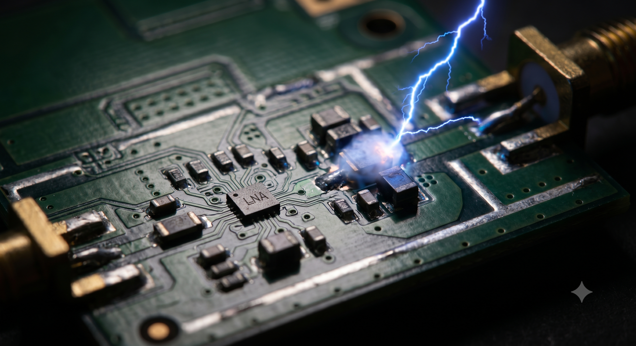
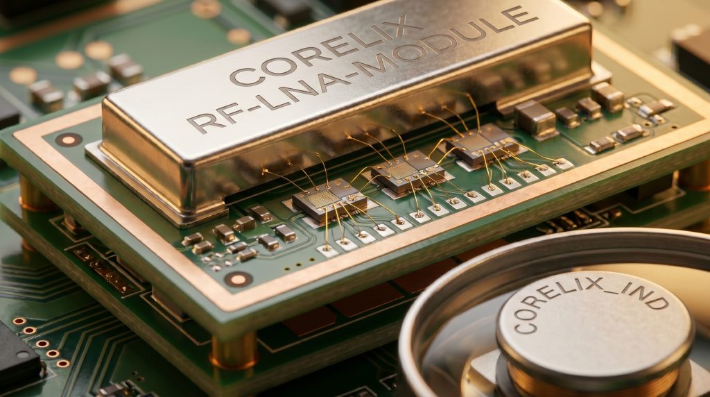
Why Does LNA Input Protection Matter?
Input protection for a Low Noise Amplifier is absolutely critical because it shields highly sensitive receiver front-ends from destructive high-power RF signals and transient voltage spikes. Without this safeguard, a single accidental overpower event can instantly destroy your receiver’s first gain stage, leading to costly system downtime. This vulnerability forces system designers to balance the desperate need for survivability with the uncompromising demand for low noise performance. Fortunately, modern integrated input-protection strategies provide a robust shield that neutralizes threat levels without compromising receiver sensitivity.
How Do You Overcome Receiver Overdrive?
When you handle high-power signals, you must deploy active or passive shielding to absorb the excess energy before it reaches the active FET gate. Here is the kicker: a single microsecond of exposure can cause irreversible thermal breakdown. To prevent this, you can implement the following:
- Shunt PIN diode limiters that react in nanoseconds.
- Series attenuators that engage during overdrive conditions.
- Gas discharge tubes for high-power transmitter leakage.
Key Takeaway: Deploying these responsive limiters ensures your system remains operational during high-stress RF surges, maintaining unbroken communication lines.
How Do ESD Transients Damage Circuits?
Electrostatic discharge transients damage circuits by inducing localized dielectric breakdown and thermal runaway in the delicate sub-micron gate oxides of the primary semiconductor. In modern RF engineering, the first-stage Low Noise Amplifier is exceptionally vulnerable to these rapid voltage spikes due to its thin oxide layers.
Why Should You Worry About ESD Spikes?
Think about it: a simple touch during assembly or an atmospheric surge on an outdoor antenna can discharge thousands of volts instantly. If you do not have inline ESD clamps, this energy will path directly through the RF port, melting the gate junction.
- Human Body Model (HBM) discharges.
- Charged Device Model (CDM) events during manufacturing.
- Lightning-induced transient surges on antenna masts.
Key Takeaway: Implementing robust ESD clamping diodes at the input stage acts as an insurance policy, preventing catastrophic field failures before they ever happen.
| Threat Type | Voltage Range | Rise Time | Primary Damage |
|---|---|---|---|
| ESD (HBM) | 500V – 4kV | < 10 ns | Gate Oxide Puncture |
| ESD (CDM) | 250V – 1kV | < 1 ns | Junction Melting |
This comparison demonstrates how ESD events present ultra-fast threats that demand sub-nanosecond response times.
What Are the Core Limiter Technologies?
The core limiter technologies consist of PIN diodes, Schottky diodes, and active field-effect transistor switches configured to shunt excess RF power to ground. Selecting the right architecture for your Low Noise Amplifier depends heavily on your specific operating frequency, power threshold, and recovery time constraints.
Which Limiter Fits Your Architecture?
Want to know the best part? You do not have to sacrifice all your signal integrity to get world-class protection if you choose the correct diode structure. You should evaluate these primary options:
- PIN Diodes: Best for high power handling and low insertion loss.
- Schottky Diodes: Perfect for low threshold clamping but lower power limits.
- FET Limiters: Highly integrable directly onto the MMIC die.
Key Takeaway: Selecting a PIN-Schottky hybrid configuration allows you to achieve both low-threshold turn-on times and high-power survivability.
| Technology | Threshold | Power Handling | Integration |
|---|---|---|---|
| PIN Diode | High (+15 dBm) | Very High (>10W) | Medium (Discrete/Hybrid) |
| Schottky | Low (0 dBm) | Low (<1W) | High (Monolithic) |
Engineers must balance these distinct threshold levels to ensure early clamping without causing unnecessary signal distortion during normal operation.
How Do PIN Diodes Safeguard Signals?
PIN Diodes safeguard signals by acting as current-controlled RF variable resistors that transition from high to low impedance when exposed to high-power RF energy. This impedance change reflects the dangerous incoming power away from the sensitive Low Noise Amplifier input terminal.
How Can You Optimize Diode Bias?
Look at it this way: a passive PIN diode relies on the RF signal itself to self-bias, which can lead to a slight delay in protection. If you use active biasing instead, you can dramatically accelerate the turn-on speed.
- Self-biased limiters: Simplest layout, zero DC power.
- DC-biased limiters: Faster switching, requires control circuitry.
- Anti-parallel pairs: Symmetric clipping for bidirectional protection.
Key Takeaway: Optimizing the bias state allows you to match the speed of the limiter to the precise damage thresholds of your downstream circuitry.
| Bias Method | Turn-on Speed | Circuit Complexity | Power Consumption |
|---|---|---|---|
| Self-Biased | Slow (10-100 ns) | Very Low | Zero |
| DC-Biased | Fast (<5 ns) | Medium | Minimal (Microamps) |
This trade-off shows that active biasing is highly recommended when protecting ultra-sensitive receivers from fast-rising pulsed radar signals.
Does Protection Degrade Noise Figure?
Yes, input protection typically degrades the overall noise figure because any component placed before the first gain stage introduces resistive insertion loss. Since every decibel of loss directly adds to the noise figure of the Low Noise Amplifier, minimizing this passive attenuation is a primary design challenge.
How Do You Minimize Noise Impact?
But there is a catch: if you try to build a bulletproof limiter, the parasitic capacitance of the diodes will degrade your high-frequency return loss. You must carefully design the matching network to integrate these parasitics. Consider these strategies:
- Use low-capacitance diodes designed for millimeter-wave bands.
- Resonate out the junction capacitance with shunt inductors.
- Place the limiter after a low-loss directional coupler if appropriate.
Key Takeaway: Selecting diodes with sub-picofarad capacitance keeps insertion loss under 0.2 dB, preserving the ultra-low noise profile of your receiver.
| Diode Capacitance | Noise Figure Penalty | Operating Band | Matching Complexity |
|---|---|---|---|
| 0.1 pF | < 0.15 dB | Up to Ka-Band | Low |
| 0.5 pF | 0.40 dB | Up to X-Band | Medium |
This data illustrates why ultra-low capacitance is the most critical metric when sourcing protection components for high-frequency systems.
What Is the Impact on Input Matching?
The impact on input matching is characterized by a shift in the input impedance (S11) caused by the parallel shunt capacitance of the protection circuitry. This impedance shift can detune the input matching network of your Low Noise Amplifier, leading to reduced gain and increased signal reflections.
How Can You Correct Impedance Shifts?
Here is the kicker: even minor layout mismatches can completely ruin your VSWR at microwave frequencies. When you design the layout, you should co-simulate the limiter diodes alongside the matching transmission lines.
- Integrate diode pads into the microstrip impedance calculations.
- Use co-planar waveguide structures to minimize parasitic ground paths.
- Implement broadband stub tuners to absorb diode capacitance.
Key Takeaway: Co-designing the protection circuit with the matching network ensures low VSWR across the entire operating bandwidth, maximizing power transfer.
| Matching Method | VSWR Performance | Bandwidth | Board Space |
|---|---|---|---|
| Lumped LC | Good | Narrow | Very Small |
| Distributed Stub | Excellent | Wide | Moderate |
Utilizing distributed matching elements provides a highly reliable method to counteract the capacitive loading of high-power limiters.
How Do You Balance Power and Speed?
You balance power and speed by selecting diode I-region thicknesses that optimize charge carrier lifetime for fast turn-on times while maintaining adequate thermal volume for energy dissipation. In the context of a high-performance Low Noise Amplifier, this trade-off defines the boundaries of your system’s survivability.
What Trade-Offs Must You Manage?
Under pressure, you might be tempted to prioritize raw power handling over everything else. But don’t jump to conclusions: a thick, slow diode will let a massive “spike leakage” through to your receiver before it fully clamps.
- Thin I-regions yield sub-nanosecond response but lower peak power.
- Thick I-regions withstand hundreds of watts but leak early transients.
- Multi-stage limiters combine thin and thick diodes for optimal balance.
Key Takeaway: Using a dual-stage limiter architecture shields your system from both fast-rising spikes and sustained high-power RF overloads.
| Limiter Stage | Turn-On Speed | Max Power Handling | Leakage Level |
|---|---|---|---|
| Single-Stage (Thick) | Slow (50 ns) | Very High (100W) | High (+25 dBm) |
| Dual-Stage (Thick + Thin) | Ultra-Fast (<1 ns) | High (50W) | Ultra-Low (+12 dBm) |
This demonstrates that a multi-stage approach is the absolute gold standard for comprehensive receiver protection without compromise.
Where Should Protection Be Positioned?
Protection should be positioned as close to the antenna input port as physically possible, ideally directly before the matching network of the first active stage. Placing it here ensures that no external energy can bypass the shield and damage the sensitive Low Noise Amplifier core.
How Do You Plan the Physical Layout?
Want to know the best part? Proper physical isolation prevents mutual coupling between the noisy input lines and the clean output stages. If you ignore physical spacing, high-power signals can radiate across the board, completely bypassing your limiter.
- Keep trace lengths between the input connector and limiter under 1 mm.
- Incorporate via picket fences to isolate high-power traces.
- Shield the entire limiter cavity to prevent radiative leakage.
Key Takeaway: Placing the limiter at the absolute front gate of your system blocks both conducted and radiated RF threats from reaching your active components.
| Placement Location | Protection Level | Noise Figure Impact | Parasitic Risk |
|---|---|---|---|
| Before Matching | Maximum | Moderate (Adds loss) | Low |
| Inside Matching | High | Low | High (Detuning) |
This highlights why placement at the front gate remains the preferred choice for rugged defense.
How Do You Test Limiter Performance?
You test limiter performance by utilizing a high-power pulsed RF source, a fast-sampling oscilloscope, and a vector network analyzer to measure leakage power, recovery time, and small-signal insertion loss. Verifying these metrics is critical to guaranteeing that your Low Noise Amplifier remains fully protected under real-world operating conditions.
Are You Testing for the Worst Case?
Believe it or not, standard continuous-wave testing does not capture the transient spike leakage that destroys receiver gates. To verify your design truly works, you must simulate realistic fault conditions.
- Measure “flat leakage” during sustained high-power RF pulses.
- Verify “spike leakage” energy using ultra-fast peak power meters.
- Calculate “recovery time” to see how fast the receiver regains full gain.
Key Takeaway: Thorough pulsed testing confirms your limiter reacts fast enough to clamp lethal transient spikes before they reach sensitive semiconductor barriers.
| Parameter Tested | Equipment Needed | Target Spec | Criticality |
|---|---|---|---|
| Spike Leakage | Fast Oscilloscope | < 15 dBm Peak | Critical |
| Recovery Time | Pulsed Signal Generator | < 1 microsecond | High |
This testing methodology ensures that any deployed protection circuit meets the rigorous standards required in high-reliability applications.
What Are the Top LNA Protection FAQs?
This section answers the most common questions regarding low-power limits, integration practices, and noise management when protecting a high-frequency Low Noise Amplifier.
Can I use a Schottky diode for high-power limiting?
No, because Schottky diodes have very thin junctions that will quickly burn out when exposed to sustained RF power levels exceeding 1 Watt. They are ideal only for low-threshold, low-power applications.
What’s the best way to reduce limiter insertion loss?
Select diodes with ultra-low junction capacitance and integrate them into a custom-tuned input impedance matching network. This minimizes signal attenuation before the first amplifier stage.
How do I know if my limiter is biased correctly?
Measure the turn-on speed and insertion loss under active and passive conditions using a pulsed RF source. Correct bias will yield sub-nanosecond clamping times without adding excessive noise.
Can I place the protection circuit after the matching network?
Yes, but doing so increases the risk of matching network component breakdown and may detune the input circuit. Placing it at the front-most connector provides the safest isolation.
How do I know if the noise figure has been compromised?
Perform a cold/hot noise source calibration using a noise figure analyzer with and without the limiter installed. Any increase in noise figure directly corresponds to the limiter’s passive insertion loss.
Protecting sensitive RF receiver chains from destructive power overloads is a critical challenge, but you do not have to design these complex defense mechanisms alone. Our advanced input-protection designs successfully eliminate high-power surges, safeguard fragile gain stages, and preserve ultra-low noise figures. If you want to elevate your system’s reliability and discover what we can do for you, contact us today to collaborate with our expert engineering team.