
The design principle of a Low Noise Amplifier focuses on amplifying extremely weak signals while adding the absolute minimum amount of internal noise to the system. You often face scenarios in satellite communications or medical imaging where a critical signal is nearly buried under the thermal noise floor. If you fail to use a specialized front-end, the internal circuitry will mask the data, leading to dropped connections or unusable diagnostics. Adopting a rigorous LNA design approach solves this by maximizing sensitivity and ensuring signal integrity from the very first stage of the receiver.

What defines the primary design role of an LNA?
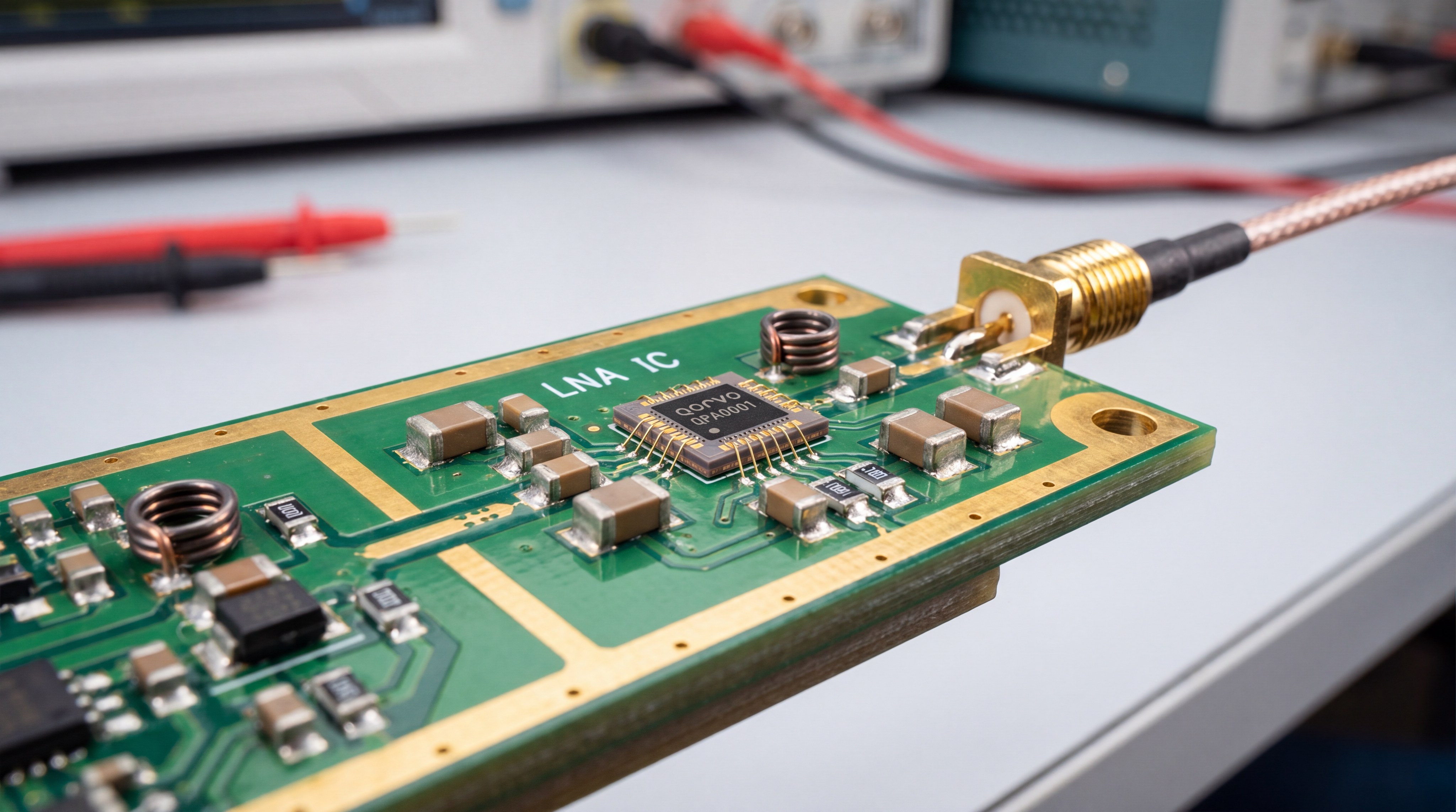
A Low Noise Amplifier serves as the gateway of any RF receiver, where its main task is to boost signal strength without degrading the signal-to-noise ratio. You must place this component as close to the antenna as possible to mitigate the noise contributions of cables and subsequent stages. This strategic placement ensures that the signal is amplified before it encounters significant losses.
How do LNAs function in the receiver section?
You will find that the LNA is responsible for setting the noise floor of the entire system. It achieves this by using high-quality transistors that exhibit very low thermal and shot noise during operation.
- Initial signal capture from the antenna.
- Immediate amplification of microvolt-level signals.
- Impedance matching to the next stage.
Here is the kicker:
Even a fraction of a decibel in noise figure improvement can significantly extend the range of your wireless system.
| Feature | Primary Function |
|---|---|
| Signal Placement | Receiver Front-End |
| Core Objective | Amplify weak signals while minimizing noise |
Properly placing the LNA at the start of your chain is the most effective way to protect weak signals from being lost.
Key Takeaway: By using an LNA as your first active stage, you ensure that the receiver sensitivity is maximized, providing the best possible foundation for data processing.
Why is noise figure minimization the most critical factor?
Noise figure minimization is the primary design objective for a Low Noise Amplifier because it determines how much “unwanted” energy is added to your signal during the amplification process. You calculate the noise figure as the ratio of the total output noise power to the output noise power due to the input source alone. A lower number represents a cleaner signal, which is essential for high-performance communication systems.
How does a lower noise figure indicate quality?
You can identify a superior LNA by its ability to maintain a noise figure typically below 2 dB in most commercial applications. This low value indicates that the internal components are highly optimized for quiet operation.
- Reduction of thermal noise from resistors.
- Selection of low-noise semiconductor materials like GaAs or GaN.
- Optimization of the input matching network.
But wait, there is more…
Lowering the noise figure directly increases the distance your receiver can successfully pick up a transmission without errors.
| Parameter | Impact on Performance |
|---|---|
| Low Noise Figure | Higher sensitivity and better signal quality |
| High Noise Figure | Signal masking and reduced communication range |
Achieving a sub-1dB noise figure is often the hallmark of world-class RF engineering.
Key Takeaway: Prioritizing a low noise figure allows you to detect signals that would otherwise be invisible, giving your hardware a competitive edge in sensitivity.

How does high gain influence LNA performance?
High gain in a Low Noise Amplifier is vital because it helps drown out the noise produced by the following components in the RF chain, such as mixers and filters. According to Friis’s Formula, the noise contribution of the second stage is divided by the gain of the first stage. Therefore, providing sufficient gain at the LNA level ensures the overall system noise figure remains low.
What is the typical gain range for an LNA?
You will typically design for a gain range between 10 dB and 30 dB depending on your specific system architecture. While more gain sounds better, you must be careful not to saturate the subsequent stages of your receiver.
- Standard gain: 15 dB to 20 dB.
- High-sensitivity gain: Up to 30 dB.
- Variable gain options for dynamic environments.
Make no mistake:
The balance between gain and stability is the most difficult tightrope you will walk during the design phase.
| Gain Level | Design Consideration |
|---|---|
| 10 dB – 30 dB | Standard range for most LNA applications |
| Over 30 dB | High risk of instability and saturation |
Managing gain effectively prevents your receiver from becoming “blinded” by its own signal strength.
Key Takeaway: Sufficient gain ensures that the noise of the rest of your system does not matter, effectively “locking in” the low-noise performance of the LNA.
Why is power consumption a major design trade-off?
Power consumption in a Low Noise Amplifier is a critical consideration, especially if you are designing for mobile devices or remote sensor nodes where battery life is a priority. You must often choose between high linearity and low current draw, as these two parameters typically pull in opposite directions. Modern designs use advanced power-saving techniques to maintain high performance without draining the system’s energy reserves.
Why select low-power consumption devices?
You choose low-power components to reduce the thermal load on your PCB, which in turn helps keep the noise figure stable. Heat is a major source of thermal noise, so a cooler-running amplifier is inherently a quieter one.
- Extended battery life for portable units.
- Lower operating temperatures for sensitive circuits.
- Reduced requirements for bulky heat sinks.
The real secret is:
Using low-power transistors doesn’t just save energy; it actually helps you maintain a lower noise floor over time.
| Design Focus | Resulting Benefit |
|---|---|
| Low-Power Devices | Reduced thermal noise and longer battery life |
| Performance Balancing | High gain without excessive current draw |
Reducing current draw is essential for modern IoT and aerospace applications where every milliamp counts.
Key Takeaway: Balancing power efficiency with performance ensures your system stays operational longer without compromising the quality of the signals you receive.
How is frequency selectivity managed in LNA circuits?
Frequency selectivity in a Low Noise Amplifier ensures that your receiver only amplifies the signals you care about while rejecting unwanted interference. In a crowded RF environment, signals from nearby cell towers or Wi-Fi routers can easily overwhelm a wideband amplifier. You implement selectivity through the use of tuned input and output networks that act as bandpass filters.
How do tuning networks reject unwanted frequencies?
You utilize inductors and capacitors to create a resonant circuit that only allows a specific range of frequencies to pass through. This prevents out-of-band signals from causing intermodulation distortion or saturating the amplifier.
- Narrowband tuning for specific protocols.
- High-Q components for sharp filter skirts.
- Integrated SAW filters for extreme rejection.
It gets even better:
Good selectivity allows you to operate in hostile signal environments where other receivers would simply fail to function.
| Frequency Type | LNA Action |
|---|---|
| Target Frequency | High-gain amplification |
| Unwanted Signal | Strong rejection and attenuation |
Focusing the amplifier’s energy only on the desired band maximizes efficiency and minimizes interference.
Key Takeaway: High selectivity protects your receiver from “blocking” signals, ensuring that your data remains clear even when the airwaves are crowded.
How do thermal variations impact design stability?
Thermal variations are a significant challenge for any Low Noise Amplifier because temperature changes directly alter the gain and noise figure of the transistor. As your hardware heats up, the random motion of electrons increases, which naturally raises the noise floor of the circuit. You must use temperature compensation techniques to ensure that your system performs consistently across its entire operating range.
How does thermal modeling prevent performance drift?
You employ advanced software to simulate how your LNA will behave at extreme temperatures, from freezing outdoor conditions to the high heat of an engine bay. This allows you to add specific components that adjust the bias current as the temperature fluctuates.
- Temperature-compensating bias circuits.
- Thermal pads for efficient heat dissipation.
- Selection of components with low thermal coefficients.
Don’t forget:
Consistency is king in professional RF systems, and thermal management is the key to that consistency.
| Thermal Factor | Mitigation Strategy |
|---|---|
| Gain Drift | Temperature-compensating bias networks |
| Noise Floor Rise | Active cooling or high-surface-area heat sinks |
Implementing thermal stability measures prevents your system from failing when the environment gets tough.
Key Takeaway: Maintaining a stable temperature environment ensures that your LNA provides predictable performance, regardless of external weather or internal heat buildup.
Why are simulations and testing vital for success?
Simulations and testing for a Low Noise Amplifier allow you to verify your design before committing to expensive hardware production. You use specialized tools to check for stability, noise figure, and S-parameters across a wide range of frequencies. This iterative process helps you find potential flaws, like oscillations, that could destroy your hardware or interfere with other nearby systems.
Why are SPICE and ADS essential for designers?
You rely on tools like ADS (Advanced Design System) to model the complex interactions of high-frequency electromagnetic waves. These simulations provide a virtual test bench where you can tweak component values in seconds rather than days.
- S-parameter analysis for impedance matching.
- Noise figure prediction based on transistor models.
- Stability factor (K-factor) calculations.
The bottom line is:
You cannot guess your way to a high-performance LNA; you must simulate, test, and verify every single parameter.
| Tool / Test Type | Primary Benefit |
|---|---|
| ADS / SPICE Simulation | Predicts performance before PCB fabrication |
| Vector Network Analysis | Verifies real-world gain and matching |
Rigorous testing is the only way to guarantee that your final product meets the demanding specs of B2B clients.
Key Takeaway: Thorough simulation and validation reduce your development risk and ensure that your LNA performs exactly as promised in the field.
How does impedance matching improve LNA efficiency?
Impedance matching is a fundamental design requirement for a Low Noise Amplifier to ensure maximum power transfer from the antenna to the amplifier. If your impedances do not match, a portion of the signal will reflect back toward the source, causing loss and increasing the noise figure. You must design the input matching network specifically for the “best noise match,” which is often different from the “best power match.”
How do transmission lines reduce noise?
You use precisely calculated transmission lines on your PCB to match the characteristic impedance of your components, usually 50 ohms. At microwave frequencies, even a tiny trace can act as an inductor or capacitor, so every millimeter of your layout counts.
- Microstrip lines for controlled impedance.
- L-match or Pi-match networks using lumped components.
- Quarter-wave transformers for narrowband matching.
Think about this:
A perfectly matched input is the difference between a high-sensitivity receiver and a piece of useless scrap metal.
| Matching Type | Design Goal |
|---|---|
| Noise Matching | Achieve the absolute lowest noise figure |
| Power Matching | Maximize signal transfer to the next stage |
Optimizing the input network for noise rather than power is the secret sauce of LNA design.
Key Takeaway: Precision impedance matching eliminates signal reflections, ensuring that every possible bit of energy from the antenna reaches the amplifier’s core.
What is the role of linearity in low noise design?
Linearity in a Low Noise Amplifier defines its ability to handle strong signals without distorting them or creating “ghost” signals called harmonics. While LNAs are built for weak signals, they must occasionally survive the presence of a strong nearby transmitter. If your amplifier is non-linear, it will mix these strong signals together, creating interference that masks the very signals you are trying to receive.
How to define linear versus non-linear operation?
You measure linearity using the 1dB compression point (P1dB) and the third-order intercept point (IP3). A higher IP3 value means your amplifier can handle larger signals before they start interfering with each other.
- Linear operation: No signal distortion.
- Non-linear operation: Clipping and harmonic generation.
- Dynamic range: The window between the noise floor and saturation.
Here is the kicker:
A high-linearity LNA is actually harder to design than a low-noise one because the two requirements often fight each other.
| Operating State | Signal Result |
|---|---|
| Linear (-60 dBm) | Clean amplification with no distortion |
| Non-Linear (0 dBm) | Signal clipping and high harmonic noise |
Ensuring your amplifier stays linear prevents data corruption during periods of high signal activity.
Key Takeaway: High linearity ensures that your receiver remains clear and functional, even when blasted by strong interfering signals from the surrounding environment.
How can you optimize noise source isolation?
Can I use an LNA as a power amplifier?
No, because LNAs are optimized for sensitivity and low noise at the input, while power amplifiers are built for high-wattage output at the end of the chain. Attempting to use an LNA for power will likely result in immediate component failure.
What’s the best way to improve my system range?
The best approach is to minimize the noise figure of your Low Noise Amplifier while ensuring the gain is high enough to overcome cable losses. This directly lowers the minimum detectable signal of your receiver.
How do I know if my LNA is oscillating?
You can identify oscillation if you see unexpected spikes on a spectrum analyzer or if the power consumption is significantly higher than the datasheet specifications. Oscillations occur when feedback paths aren’t properly managed in the PCB layout.
What’s the best frequency range for a standard LNA?
The best range depends entirely on your application, but most standard platforms cover from 30 MHz up to 6 GHz for common communications. High-frequency versions can extend well into the millimeter-wave bands for satellite use.
How do I know if my design is thermally stable?
You should monitor the gain and noise figure while cycling the hardware through its intended temperature range in an environmental chamber. Consistent data across all temperatures indicates a successful, thermally-compensated design.
Developing a high-performance receiver doesn’t have to be a guessing game. By mastering these design principles—from noise figure minimization to impedance matching—you can build systems that thrive in the most challenging electromagnetic environments. Whether you need a standard module or a complex, high-frequency integration, our engineering team is ready to help you move from requirement review to validated delivery. If you are ready to elevate your RF project with factory-direct precision, contact us today to start a technical discussion.
CorelixRF: Engineering the path from chip-level design to system-level RF excellence.