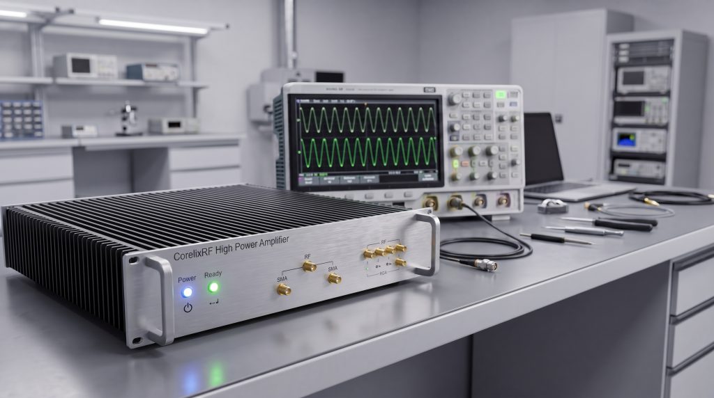
The core applications and technical benefits of CorelixRF High Power Amplifiers in modern RF systems lie in their ability to balance high-efficiency power output with exceptional signal linearity across demanding telecommunications, defense, and satellite communication channels.
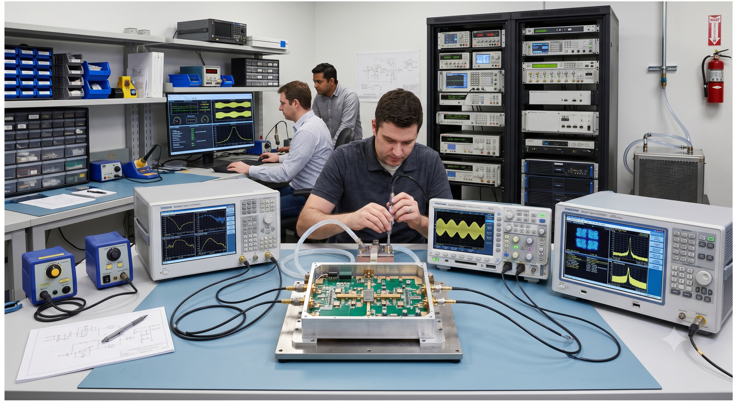
An RF engineering team is preparing to validate a high-power broadband transmitter system on the laboratory bench. All of the signal source hardware, digital modulations, and spectral analyzers are perfectly calibrated and ready for testing. Suddenly, the team hits a massive roadblock during initial active component testing.
Traditional amplifier designs force a brutal, unacceptable choice: use Class A architectures that deliver high signal linearity but waste over seventy percent of their energy as heat, or implement Class B systems that boost efficiency but introduce destructive crossover distortion. A CorelixRF High Power Amplifier resolves this engineering dilemma by biasing active components to operate between 180 and 360 degrees of the input signal. This precise configuration delivers the high power efficiency of Class B architectures alongside the exceptional signal linearity of Class A layouts, making them the absolute industry standard for modern, high-reliability RF systems.
Why Choose CorelixRF for High Power Amplification?
Class AB is the optimal design choice for high power amplification because it successfully bridges the gap between high operational efficiency and low signal distortion. Integrating a Class AB High Power Amplifier into your system prevents the extreme thermal losses associated with Class A configurations while maintaining high signal purity.
This design allows RF engineers to meet strict regulatory spectral masks without requiring excessively large power supplies. It remains the industry-standard topology for modern, high-reliability transceiver front ends.
What is the Fundamental Class AB Design?
This fundamental design is established by setting the conduction angle of the active transistors to operate between 180 and 360 degrees of the input signal cycle. By setting the gate bias voltage slightly above the transistor’s cutoff threshold, you ensure a small amount of idle current flows constantly. This idle current keeps the devices active during zero-crossing periods, which effectively eliminates the dead zone that causes severe waveform distortion in pure Class B setups.
Let me explain:
- The transistor operates in its linear region for over half of the cycle.
- The continuous bias prevents sharp turn-on transients on your waveform.
- This configuration balances power savings with signal accuracy.
You can rely on this setup to keep your transmitter outputs stable.
How Does It Compare to Class A and Class B?
When comparing topologies, Class A amplifiers offer absolute linearity but operate at an extremely low power efficiency of around twenty-five percent. Class B systems boast high efficiency up to seventy-eight percent but generate high levels of crossover distortion. Class AB strikes a perfect balance, delivering up to sixty percent power-added efficiency alongside exceptional linearity.
Think about it:
- Class A wastes enormous amounts of standby energy as heat.
- Class B introduces distortion that corrupts high-order digital modulations.
- Class AB minimizes thermal stress while preserving signal constellations.
You get a clean, reliable output without draining your power budget.
Key Takeaway: Choosing a Class AB design allows B2B buyers to optimize their system power budgets and physical size constraints without risking signal degradation or costly spectral mask violations.
| Parameter / Feature | Class A | Class B | Class AB |
|---|---|---|---|
| Conduction Angle | 360 degrees | 180 degrees | 180 to 360 degrees |
| Max Efficiency | ~25% – 50% | ~78.5% | ~50% – 65% |
| Crossover Distortion | Zero | High | Negligible |
To manage this balance between linearity and efficiency, designers must pay close attention to active biasing networks.
How Does Class AB Improve Efficiency and Linearity?
Class AB improves efficiency and linearity by utilizing precise biasing that shuts down active stages during low-signal periods while maintaining a smooth waveform transition. Implementing a High Power Amplifier with this configuration ensures your transmitter operates at peak energy efficiency without distorting the signal path.
This dynamic capability prevents your system from wasting valuable energy as heat during standby states. Consequently, your operational costs drop while the overall reliability of the semiconductor components rises.
Why Is Biasing Critical for Linear Performance?
Active biasing is critical because it dictates the exact transition point where your transistors shift from cutoff to active conduction. If the bias voltage drifts, your amplifier will quickly slip into highly distorted Class B operation or highly inefficient Class A behavior. You must utilize temperature-compensated bias networks to keep this threshold stable under changing operating loads.
Look at these facts:
- Gate-source voltage must be tightly regulated against thermal drift.
- Minor voltage fluctuations can cause severe intermodulation spikes.
- Active biasing maintains a steady idle current under fluctuating loads.
How does this work? Active temperature compensation circuits monitor the physical environment to adjust gate voltages in real-time.
Can We Eliminate Intermodulation Distortion?
While complete physical elimination of intermodulation distortion is impossible, you can suppress it to negligible levels using advanced linearization techniques. Implementing analog predistortion or digital predistortion (DPD) alongside a balanced push-pull Class AB layout allows you to cancel out third-order intermodulation products. This maintains high signal-to-noise ratios across wide bands.
Here is the truth:
- Balanced push-pull circuits naturally cancel out even-order harmonics.
- Linearization algorithms actively pre-distort the input signal to cancel phase errors.
- These combined methods push unwanted distortion products far below the noise floor.
You will achieve an incredibly clean spectrum that easily passes stringent certification audits.
Key Takeaway: Suppressing intermodulation distortion ensures that your system meets strict adjacent channel leakage ratio (ACLR) standards, protecting you from costly deployment delays and regulatory compliance failures.
| Linearization / Biasing Metric | Without Correction | With Active Predistortion | B2B Operational Impact |
|---|---|---|---|
| IMD3 Suppression | -30 dBc | -50 dBc or better | Cleaner spectrum, higher capacity |
| Spectral Regrowth | High at saturation | Minimized near compression | Compliance with FCC/CE masks |
| Bias Stability | Drift-prone | Highly stable | Predictable field behavior |
Once these linear performance levels are locked in, these amplifiers are ready for deployment in complex cellular networks.
Where Are These Amplifiers Used in Modern Telecom?
These amplifiers are widely used in modern telecom networks to power 5G base stations, macrocells, and long-range point-to-point microwave links. Selecting a Class AB High Power Amplifier enables service providers to transmit highly complex, multi-carrier data streams across wide geographical areas with minimal power drop-offs.
Their excellent handling of high peak-to-average power ratios makes them the standard choice for next-generation telecom. Consequently, modern networks can support massive subscriber counts without experiencing dropouts.
How Do Amplifiers Support 5G Infrastructure?
5G networks utilize complex orthogonal frequency-division multiplexing (OFDM) schemes that produce high peak-to-average power ratios. You need amplifiers that can handle these sudden power surges without clipping the signal peak. Class AB systems are specifically engineered to provide linear amplification across wide instantaneous bandwidths.
Here is the deal:
- Wide bandwidth support allows for multi-carrier aggregation.
- High peak power capability prevents digital signal clipping.
- Low noise figures preserve signal quality at the cell edge.
You will find that these features keep your 5G throughput at maximum speed.
What Role Do They Play in Cellular Base Stations?
Base stations operate continuously under varying subscriber loads, requiring highly efficient and reliable power delivery. The Class AB output stage provides the essential drive power required to send signals to the edge of the cell coverage area. When you integrate these systems, you significantly reduce overall power consumption at the site.
But wait, there is more:
- They dynamically scale current draw based on real-time traffic demand.
- They support massive MIMO antenna arrays with modular configurations.
- They survive harsh outdoor environments within sealed equipment housings.
You can easily deploy these modules to guarantee high network availability and minimal downtime.
Key Takeaway: Utilizing Class AB modules in base stations lowers your operational electricity bills by up to thirty percent while maintaining pristine voice and data signal coverage for end-users.
| Base Station Requirement | Class AB Solution | Practical Customer Benefit |
|---|---|---|
| High PAPR Signals | High peak power capability | No digital signal distortion |
| Continuous Operation | Dynamic bias adjustments | Lower thermal load and power bills |
| Cell Edge Coverage | Stable high-gain output | Reduced dropped connections |
To achieve these strict telecom standards, the underlying semiconductor technology must provide exceptional power density and thermal conductivity.
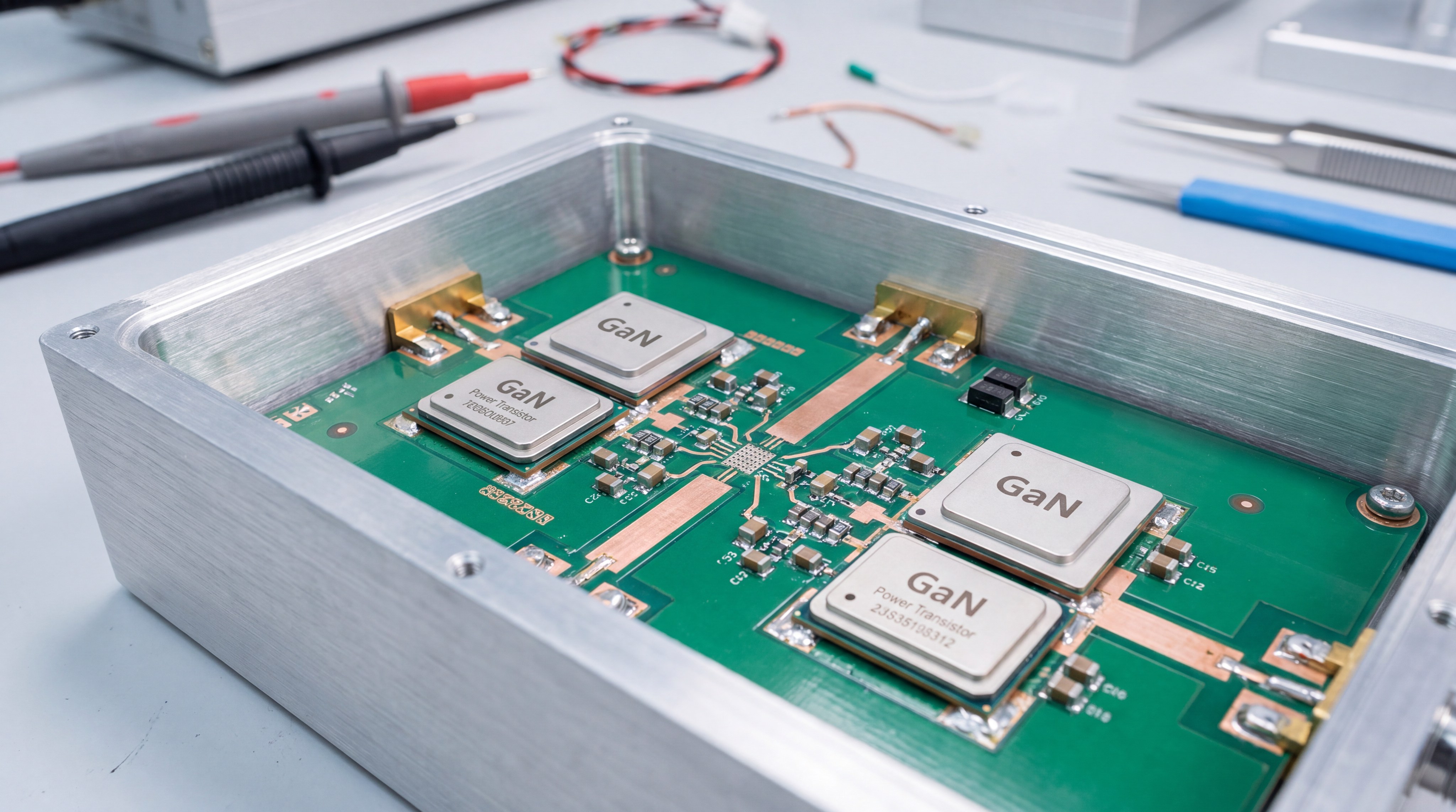
What Makes GaN Ideal for Class AB RF Amplifiers?
GaN is ideal for Class AB configurations because of its exceptionally high breakdown voltage, superior power density, and excellent thermal conductivity. By utilizing a GaN-based High Power Amplifier, you can shrink your overall system size while dramatically increasing output power.
These advanced wide-bandgap transistors allow systems to operate at much higher temperatures than traditional silicon components. This makes them perfect for ruggedized field deployments where external cooling options are highly limited.
Why Use Gallium Nitride Over Silicon LDMOS?
Gallium Nitride (GaN) provides up to ten times the power density of traditional silicon laterally diffused metal-oxide-semiconductor (LDMOS) technology. This physical advantage means you can achieve the same RF output power using a much smaller active device area. Consequently, your parasitic capacitance drops, allowing for wider operational bandwidths.
Look at these facts:
- GaN operates at much higher frequencies than silicon LDMOS.
- The material exhibits higher saturated electron velocity.
- Drain efficiency remains high even at high operational frequencies.
Think about it: smaller packages mean lighter payloads for your tactical mobile applications.
How Does GaN Handle High Operating Voltages?
GaN’s wide bandgap energy allows the semiconductor to withstand high electric fields without suffering from avalanche breakdown. This capability permits the device to run at operating voltages of 48 volts or higher, which is double that of typical silicon devices. You can leverage this high voltage to reduce current draw and simplify power distribution networks within your system.
Let me explain:
- High voltages reduce conduction losses along your power rails.
- The system handles sudden power spikes without experiencing breakdown.
- Your power supply units can be built with smaller, lighter components.
You will achieve maximum reliability even under unstable field voltage conditions.
Key Takeaway: Incorporating GaN-based amplifiers reduces overall system weight and power routing complexity, offering B2B buyers major savings in transportation and assembly costs.
| Physical Parameter | Silicon LDMOS | Gallium Nitride (GaN) | System Impact |
|---|---|---|---|
| Power Density | Low (~1-2 W/mm) | Very High (~10-20 W/mm) | Extremely compact transmitter sizes |
| Breakdown Voltage | ~70V – 80V | 150V or higher | Higher operating safety margins |
| Bandgap Energy | 1.1 eV | 3.4 eV | Reliable high-temperature performance |
However, harvesting these immense power levels from compact semiconductors requires a world-class approach to thermal dissipation.
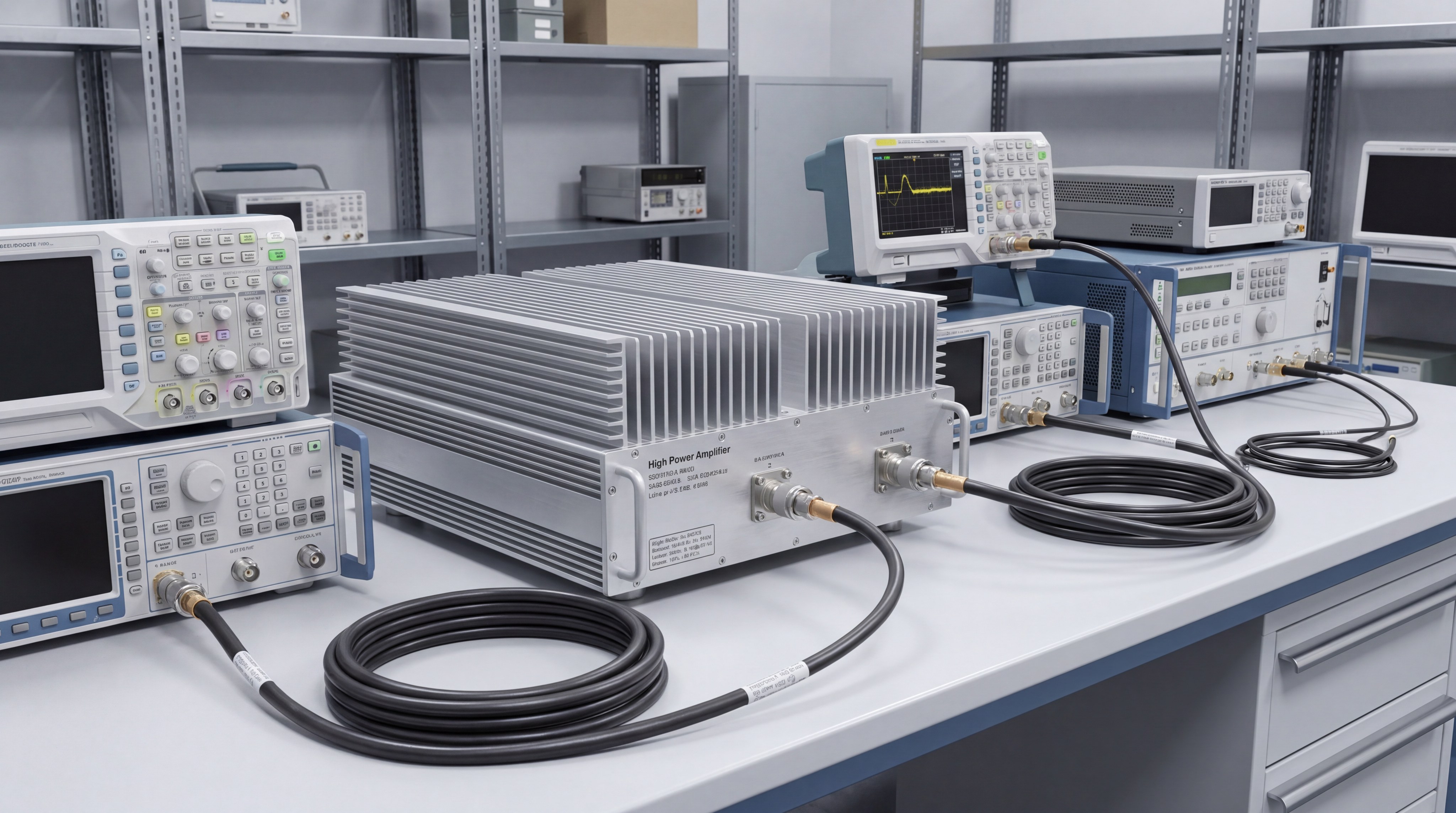
How Do You Manage Thermal Dissipation in RF Systems?
You manage thermal dissipation in high-power RF systems by using a structured combination of high-conductivity heat spreaders, high-performance passive heatsinks, and forced-air or liquid cooling mechanisms. Integrating these thermal solutions with your Class AB High Power Amplifier prevents localized hot spots and ensures long-term semiconductor reliability.
Without effective thermal management, your amplifier will experience rapid gain degradation and premature physical failure. Implementing robust cooling layouts keeps junction temperatures well within safe limits during continuous-wave operations.
What Are the Best Active Cooling Methods?
Forced-air cooling using high-reliability brushless fans remains the most common active method for rack-mounted systems. These fans draw cool air across optimized copper or aluminum heatsink fins to carry away waste heat. You should implement speed-controlled fans that adjust their airflow dynamically based on real-time temperature sensors.
Here is the truth:
- Active airflow increases dissipation capacity by up to five times.
- Dynamic speed controls reduce environmental acoustic noise.
- Redundant fan layouts protect the system from individual fan failures.
In other words, smart cooling keeps your maintenance costs to a minimum.
How Do Liquid-Cooled Systems Keep Amps Safe?
For multi-kilowatt transmitter systems, liquid cooling provides the ultimate thermal transfer efficiency. By routing a coolant mixture through a dedicated cold plate mounted directly beneath the RF modules, you can transfer massive heat loads away instantly. This closed-loop design eliminates the need for loud, high-volume air blowers inside your clean laboratory environment.
How does this work?
- A pump continuously circulates coolant through the internal copper pipes.
- The liquid absorbs heat from the amplifier blocks with zero air drag.
- An external heat exchanger dissipates the energy safely away from your rack.
You get a completely silent, high-efficiency system that handles extreme duty cycles with ease.
Key Takeaway: Liquid cooling provides maximum thermal stability for ultra-high-power installations, ensuring B2B operations run continuously without thermal throttling or hardware shutdowns.
| Cooling Approach | Thermal Dissipation | System Complexity | Ideal B2B Use Case |
|---|---|---|---|
| Passive Heatsink | Low to Moderate | Very Low | Remote, unmanned outdoor enclosures |
| Forced-Air Cooling | High | Moderate | Indoor telecom server racks |
| Liquid Cold Plate | Extremely High | High | Multi-kilowatt defense radar sites |
Alongside thermal management, achieving proper electromagnetic impedance matching is equally critical to prevent energy from reflecting back as heat.
Why Is Impedance Matching Critical for RF Amps?
Impedance matching is critical for RF amplifiers because it ensures maximum power transfer from the active transistor stage to the antenna while preventing destructive signal reflections. Integrating a High Power Amplifier with perfectly matched input and output networks is essential for protecting your system from high voltage standing wave ratio (VSWR) damage.
Proper impedance transformation minimizes insertion losses and stabilizes the operational gain across your target bandwidth. Consequently, your system maximizes its overall power-added efficiency (PAE) and signal range.
What is the Function of Microstrip Lines?
Microstrip lines act as high-precision transmission structures etched onto the printed circuit board to guide RF signals between components. You can design these lines with specific trace widths and dielectric materials to establish a precise fifty-ohm characteristic impedance. This structure prevents signal attenuation and phase distortion along the critical RF signal path.
Think about it:
- Microstrip dimensions control characteristic impedance.
- They provide low-loss transitions between active stages.
- Precise spacing minimizes cross-talk and parasitic coupling.
How do we achieve this? Designers use electromagnetic simulation software to model PCB traces perfectly before manufacturing.
How Do Stub Tuners Minimize Signal Reflection?
Stub tuners introduce short-circuited or open-circuited transmission line segments parallel to the main signal path to cancel out reactive impedance components. By adjusting the length and position of these stubs, you can match highly complex loads to the amplifier’s optimal output impedance. This precise tuning minimizes signal reflections and prevents dangerous voltage spikes from degrading your transistors.
But wait, there is more:
- They allow you to optimize impedance match at specific frequencies.
- They provide a physical means to compensate for load variations in the field.
- They maximize power transfer to your antenna system under all conditions.
You will achieve an exceptionally low return loss that guarantees your signal makes it to its destination.
Key Takeaway: Implementing high-precision stub tuning maximizes signal transmission efficiency, ensuring B2B buyers get full value out of their high-power hardware.
| Matching Component | Primary Technical Function | Operational Bandwidth | Physical Footprint |
|---|---|---|---|
| Microstrip Lines | Fixed impedance routing | Wideband | Integrated on PCB |
| Stub Tuners | Reactive impedance cancellation | Narrowband (Tuneable) | Medium external component |
| Lumped Elements | Low-frequency matching | Moderate | Extremely compact |
Achieving high impedance match stability is particularly critical in severe defense and aerospace environments.
What Are the Key Applications in Defense and Radar?
The key applications in defense and radar include high-performance active electronically scanned arrays (AESA), electronic countermeasure (ECM) jamming platforms, and secure military communication transceivers. Implementing a Class AB High Power Amplifier in these defense systems ensures that your tactical signals remain powerful and clear over long ranges.
These rugged amplifiers are engineered to survive extreme shock, high vibration, and wide temperature swings. Their ability to deliver high peak power is vital for target detection and electronic warfare success.
Why Do Military Radars Need High Peak Power?
Military radar systems must transmit short, high-energy RF pulses to detect small or stealthy targets at extreme distances. You need amplifiers that can transition from silent standby states to maximum saturated output power in nanoseconds. Class AB systems handle these high peak currents with minimal pulse distortion or thermal overshoot.
Look at these facts:
- High peak power improves radar target resolution.
- It extends the maximum effective detection range.
- Pulsed operation keeps average thermal load low.
But wait, there is more: these pulsed systems require fast gating controls to synchronize transmissions perfectly.
How Do Amplifiers Resist Electronic Jamming?
Electronic warfare environments are filled with hostile jamming signals designed to overwhelm military communications. You can resist these threats by using amplifiers with ultra-wideband coverage and high linearity to support rapid frequency-hopping spread spectrum (FHSS) schemes. This agility allows your communication links to jump across frequencies before jammer systems can lock onto them.
In other words:
- Broadband coverage lets you exploit clear frequencies instantly.
- High linearity prevents self-interference during hopping.
- Robust output power overrides weak tactical jammers.
You will keep your critical data pipelines open when it matters most.
Key Takeaway: High-power broadband linearity protects critical defense communication links, providing tactical commanders with secure and reliable data flow during active jamming operations.
| Defense / Radar Need | Class AB Capability | Operational Advantage |
|---|---|---|
| Target Detection | High peak power pulses | Extended radar detection range |
| Electronic Jamming | Ultra-wideband frequency agility | Resilience to hostile signal blocking |
| Harsh Battlefield | Ruggedized package design | Survival under extreme physical vibration |
High-reliability standards are similarly demanded when launching RF equipment into space-based satellite orbits.
How Do High Power Amplifiers Perform in Satellite Tech?
High power amplifiers perform exceptionally well in satellite technology by delivering the high gain and power-added efficiency required to transmit signals through the Earth’s atmosphere. Deploying a Class AB High Power Amplifier within your satellite payload allows you to maintain stable uplink and downlink connections while minimizing solar power draw.
These space-qualified systems are specifically shielded to withstand intense radiation and extreme vacuum environments. Their reliable operation is critical for deep-space exploration and global telecommunication networks.

What Are the Challenges of Space Environments?
Space environments present extreme engineering challenges, including cosmic radiation, thermal vacuums, and zero convection cooling. You must design your amplifiers to rely purely on conductive heat paths to transfer heat to the satellite’s outer radiant panels. Any component failure in orbit is catastrophic, as physical repair or replacement is impossible.
Here is the deal:
- Radiation can cause single-event latchups in semiconductors.
- Vacuum conditions lead to outgassing of standard materials.
- Thermal cycling spans hundreds of degrees in orbit.
Think about it: choosing space-grade, hermetically sealed components is mandatory for your mission’s success.
How Do Solid State Power Amplifiers Help Satellites?
Solid-state power amplifiers (SSPAs) have largely replaced traditional traveling wave tube amplifiers (TWTAs) in modern low-Earth orbit satellites because of their superior reliability and lower operating voltage. You can use SSPAs to gain fine-grained control over signal phase and amplitude across multiple active antenna elements. This capability enables dynamic beamforming to focus signal coverage on high-demand geographical zones.
Let me explain:
- Solid-state designs offer soft-fail characteristics compared to catastrophic tube failures.
- Lower operating voltages reduce your risk of internal electrical arcing in a vacuum.
- Phased arrays allow you to redirect beams without physical thrusters.
You will achieve unprecedented mission lifetime and flexible coverage profiles.
Key Takeaway: Utilizing solid-state technology increases satellite payload life to fifteen years or more, shielding B2B operators from premature satellite replacement costs.
| Technology | Reliability Rating | Operating Voltage | Beamforming Support |
|---|---|---|---|
| Traveling Wave Tube | High risk of filament wear | Thousands of Volts | Hard to implement |
| Solid-State SSPA | Exceptionally High | 28V to 48V | Excellent (Phased Arrays) |
| Hybrid Networks | Moderate | Mixed | Fair |
Whether deployed in orbit or on the ground, all amplifiers must undergo exhaustive lab testing before field deployment.
What Are the Standard Testing Methods for RF Amps?
The standard testing methods for RF amplifiers involve a comprehensive suite of measurements including S-parameters, Power-Added Efficiency, Error Vector Magnitude, and spectral harmonic analysis. Utilizing these tests on your Class AB High Power Amplifier guarantees that the unit meets all specified datasheet parameters before system integration.
These standard validation procedures identify any manufacturing variations or marginal component behaviors. Consequently, you can resolve potential field performance issues during the early laboratory phase.
What Is Error Vector Magnitude Testing?
Error Vector Magnitude (EVM) testing measures the physical difference between the ideal modulated signal and the actual measured output of your amplifier. A high EVM value indicates phase noise or amplitude distortion that will corrupt your digital data streams. You must keep EVM percentages exceptionally low to support high-order modulations like 256-QAM in modern networks.
Let me explain:
- EVM reflects the total signal path modulation quality.
- In-band distortion directly degrades EVM scores.
- Low EVM ensures high data throughput for users.
How does this work? High-precision vector signal analyzers compare the IQ constellation points in real-time.
How Do Spectrum Analyzers Verify Harmonics?
Spectrum analyzers display signal amplitude across a wide frequency span to verify that harmonic products remain below strict regulatory limits. When testing Class AB systems, you must check the second and third harmonics to ensure they are suppressed far below your carrier level. This verification ensures your transmitter does not bleed energy into neighboring communication bands.
Think about it:
- Unchecked harmonics interfere with surrounding channels.
- You must verify harmonic levels at saturated output power.
- Proper filter networks are designed based on these analyzer sweeps.
You will ensure your designs comply with international spectral emission regulations.
Key Takeaway: Verifying harmonic compliance protects B2B operations from regulatory fines and ensures seamless integration with adjacent radio systems in busy spectral environments.
| Measurement Parameter | Primary Test Instrument | Target Value Range | Technical Purpose |
|---|---|---|---|
| EVM (Modulation) | Vector Signal Analyzer | < 2% (For high-order QAM) | Verify digital signal quality |
| Harmonics | Spectrum Analyzer | < -45 dBc | Ensure regulatory compliance |
| S-Parameters | Vector Network Analyzer | Flat gain across band | Validate input/output match |
With exhaustive test data in hand, you can confidently proceed to select the ideal hardware configuration for your application.
How Do You Select the Right Amplifier for Your Needs?
You select the right amplifier for your needs by carefully matching your target frequency range, continuous and peak power requirements, thermal budget, and control interface parameters to your application’s physical environment. Choosing a Class AB High Power Amplifier from an experienced manufacturer ensures you receive a pre-validated design that minimizes your development risks.
This structured selection process prevents you from over-specifying performance metrics and over-spending your project budget. Let’s look at how to balance these complex engineering criteria.
How to Balance Cost and Performance Metrics?
Balancing cost and performance requires identifying which parameters are non-negotiable and which have design margins. For instance, while GaN provides ultimate high-frequency performance, silicon LDMOS may be much more cost-effective for sub-gigahertz systems. You should partner with direct factory engineers to analyze these tradeoffs before finalizing your procurement specification.
Consider these operational benefits:
- LDMOS reduces initial hardware acquisition costs.
- GaN maximizes efficiency to lower long-term power bills.
- Standard module form factors eliminate custom engineering fees.
Best of all, direct factory sourcing removes middleman markups from your purchase.
What Customization Options Are Available?
Leading manufacturers offer extensive customization options, including specialized RF connectors, modified chassis dimensions, alternative supply voltages, and tailored gain profiles. You can collaborate directly with engineering teams to modify standard platforms to fit your precise mechanical envelope or cooling systems. This hybrid approach delivers a bespoke solution with the rapid delivery times of a standard product.
In other words:
- You get an exact mechanical fit for your existing rack systems.
- Custom gain stages match your specific signal generator outputs.
- Unique connector layouts simplify your internal cable routing.
You can bypass the high cost of custom clean-sheet engineering.
Key Takeaway: Customizing standard platforms allows B2B buyers to secure exact mechanical and electrical fits without paying the extreme development costs of clean-sheet designs.
| Selection Criterion | Standard Platform | Customized Platform | B2B Procurement Strategy |
|---|---|---|---|
| Lead Time | 1 to 2 Weeks | 4 to 6 Weeks | Standard for speed, custom for fit |
| NRE Cost | Zero | Minimal | Maximize budget efficiency |
| Enclosure Fit | Fixed dimensions | Modified physical housing | Seamless system integration |
Having chosen your ideal technical specifications, it is time to look at the overall path forward for your system design.
Conclusion
Modern RF transmitter designs no longer have to compromise on signal linearity to achieve high electrical efficiency. Class AB high power amplifiers successfully resolve this classic engineering trade-off by operating with an optimal conduction angle that eliminates crossover distortion while keeping thermal dissipation highly manageable. Whether you are building next-generation 5G base stations, rugged defense radar systems, or space-bound satellite payloads, selecting a reliable active stage is paramount to your project’s overall field success.
At CorelixRF, we leverage over thirty years of deep RF engineering and manufacturing experience to design, validate, and deliver high-performance Class AB platforms directly from our state-of-the-art facility. From chip-level GaN integration to complete turnkey, liquid-cooled rack-mount subsystems, our factory-direct model guarantees that you receive unit-level tested hardware with certified data sheets before deployment. Our long-term brand vision is to empower engineering teams worldwide with the most advanced, highly reliable, and easily customizable RF amplification platforms in the industry. To discuss your specific frequency, power, and environmental requirements with a senior engineer or to request a detailed technical review, please contact us today.
FAQ
Can I customize a Class AB amplifier for pulsed radar setups?
Yes, you can. Modern Class AB systems can be optimized for high-power pulsed operations by modifying internal gate biasing networks and adding fast TTL gating controls. This allows the amplifier to support peak power levels reaching up to tens of kilowatts with microsecond rise and fall times.
What’s the best semiconductor for GHz high-power systems?
Absolutely, Gallium Nitride (GaN) is the undisputed industry standard. GaN’s high breakdown voltage and superior power density allow it to run at higher operating voltages, delivering exceptional efficiency and massive bandwidth compared to traditional silicon designs.
How do I know if my system needs coaxial SMA or N-type?
It depends on your continuous power levels and frequency range. You should choose N-type connectors for systems operating below ten gigahertz at power levels exceeding two hundred watts, whereas SMA connectors are ideal for compact, high-frequency, lower-power configurations.
Can I run these high power amplifiers without forced cooling?
No, you cannot. High power systems operating in Class AB still generate considerable heat that must be continuously dissipated. Running these modules without a properly sized passive heatsink, forced-air fan, or liquid-cooled plate will cause rapid thermal runaway and permanent hardware damage.
How do I know if my input signal is too high for the amplifier?
You should monitor the input power level against the specified 1dB compression point. If your input signal drives the amplifier deep into saturation, you will notice a sharp drop in gain flatness, high EVM degradation, and massive spectral regrowth in adjacent channels.