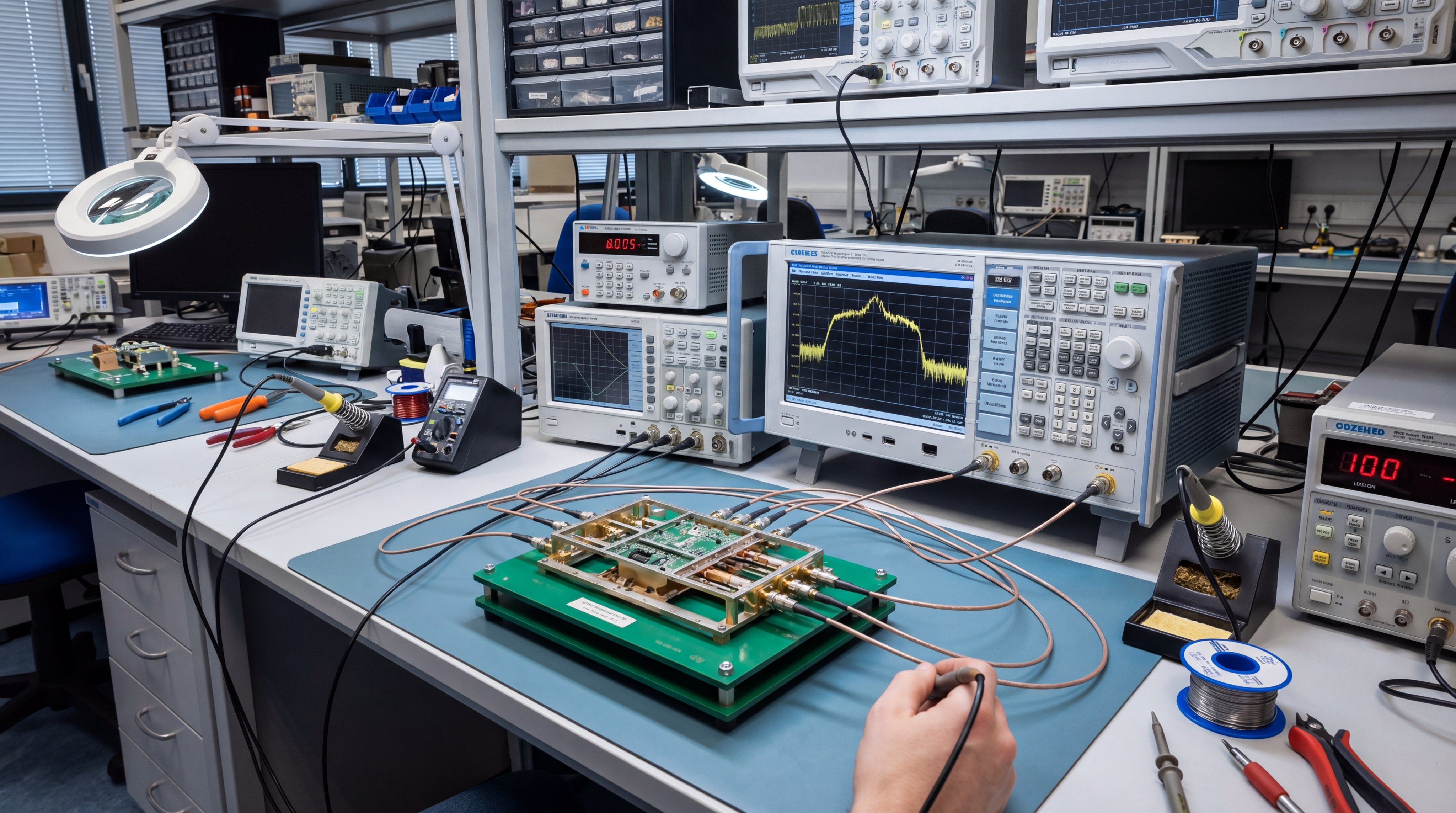
RF PCB layout represents the fundamental framework for ensuring high-frequency signal integrity and power stability in modern electronic systems. Engineers often struggle with unexpected signal degradation or interference that only appears once a physical board is fabricated. This leads to costly redesign cycles, missed project deadlines, and hardware that fails to meet stringent spectral masks. By applying rigorous layout standards for transmission lines and power delivery, you can transform a volatile prototype into a stable, high-performance RF Power Amplifier solution from Corelix RF.
Why is RF PCB layout critical for performance?
The success of an RF Power Amplifier depends entirely on how the physical traces and layers are organized on the circuit board. At high frequencies, every millimeter of copper acts as an inductor or a capacitor, potentially altering the signal in ways a schematic cannot predict. Proper layout prevents these parasitic elements from distorting the waveform.
Maintaining signal purity?
Keeping signals clean requires a deep understanding of how energy travels through the substrate.
Think about it.
- Uncontrolled return paths create ground loops.
- Return paths inject noise into the signal chain.
- Signal purity depends on consistent ground reference.
Reducing parasitic effects?
Parasitic capacitance between traces can cause crosstalk that ruins isolation between channels.
It gets better.
- Proper spacing minimizes unintended interactions.
- Guard traces can improve channel isolation.
- Component orientation impacts mutual coupling.
Key Takeaway: A well-executed layout is the only way to ensure that theoretical performance translates into real-world reliability.
| Layout Element | Impact on Performance | Mitigation Strategy |
|---|---|---|
| Trace Length | Signal Attenuation | Keep RF paths as short as possible |
| Trace Spacing | Mutual Coupling | Increase distance and use guard traces |
| Ground Planes | Return Path Discontinuity | Maintain a solid reference plane |
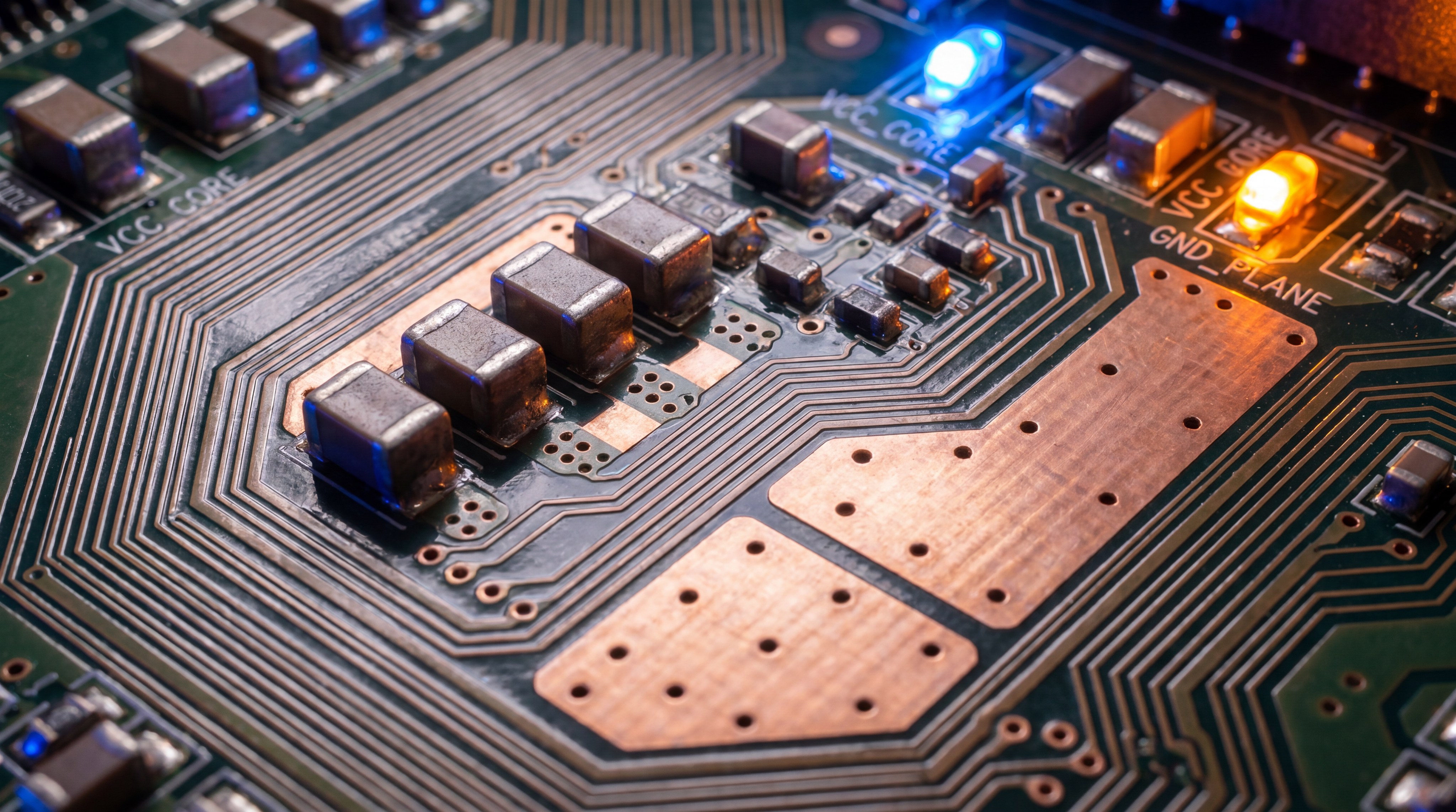
How does PDN design impact signal integrity?
The power delivery network provides the energy necessary for an RF Power Amplifier to operate without introducing spectral regrowth. If the PDN is poorly designed, it can act as an antenna, radiating noise across the board and into sensitive analog blocks. A stable PDN is non-negotiable for low-noise applications.
Minimizing ground bounce?
Ground bounce occurs when large current spikes cause the reference voltage to fluctuate.
Here is the thing.
- Fluctuations trigger false logic states.
- Noise distorts amplification stage bias levels.
- Low-impedance planes reduce voltage spikes.
Star routing techniques?
Star routing involves connecting each power-hungry component to a central supply point via individual traces.
This prevents noise leakage.
- Independent traces isolate sensitive supply pins.
- Centralized points ensure uniform voltage delivery.
- Iterative routing improves linear operation stability.
Key Takeaway: Robust power delivery is just as important as signal routing for maintaining a clean output spectrum.
| PDN Feature | Primary Benefit | Common Challenge |
|---|---|---|
| Star Routing | Isolation between stages | Increased trace congestion |
| Power Planes | Low impedance delivery | Potential for EMI radiation |
| Local Regulation | Stable bias voltages | Heat dissipation requirements |
What are the best practices for line routing?
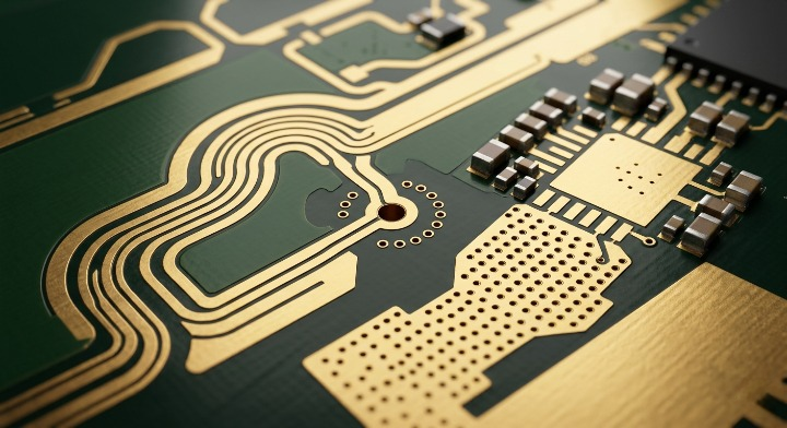
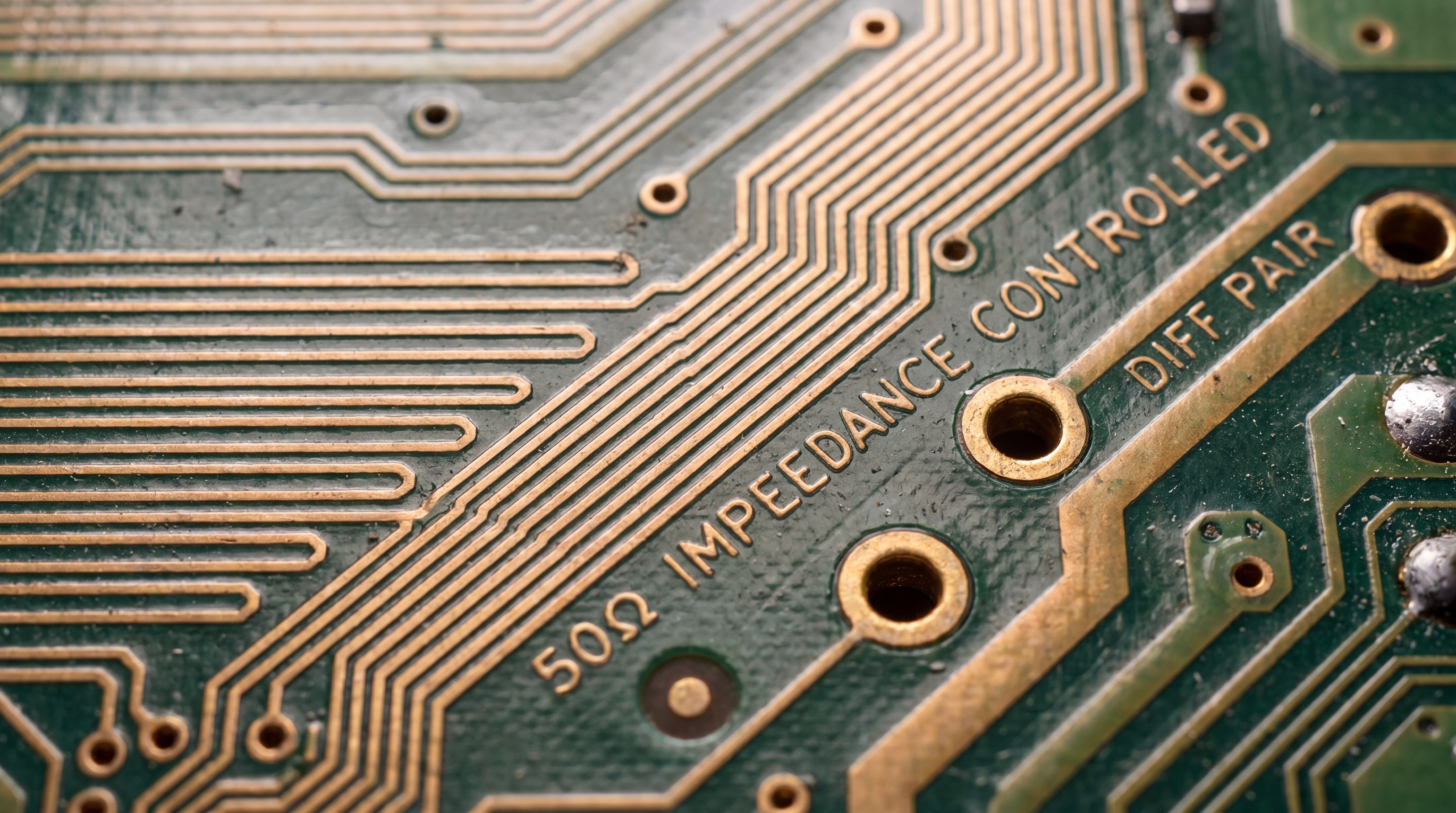
Routing a transmission line for an RF Power Amplifier requires strict adherence to 50-ohm impedance standards to prevent signal reflections. Any change in trace width or a sharp bend in the path can create an impedance mismatch that degrades the Voltage Standing Wave Ratio. Consistent geometry is the goal for every RF trace.
Stripline vs Microstrip?
Microstrip routing on the top layer is convenient for assembly but can radiate energy more easily.
Stripline routing offers superior shielding.
- Buried traces provide inherent isolation.
- Microstrips allow for easy component integration.
- Layer choice depends on target frequency limits.
Avoiding sharp bends?
Sharp 90-degree corners create a change in the effective width of the trace, leading to parasitic capacitance.
Let’s dive in.
- Mitered bends reduce impedance discontinuities.
- Smooth curves prevent signal reflections.
- Constant width ensures stable wave propagation.
Key Takeaway: Smooth, consistent trace geometry is the foundation of a high-performance RF signal path.
| Route Type | Impedance Control | Shielding Level |
|---|---|---|
| Microstrip | Excellent | Moderate |
| Stripline | Superior | High |
| Coplanar | Flexible | Good |
How do you manage impedance vs manufacturing?
Engineers must reconcile the theoretical needs of an RF Power Amplifier with physical limitations of the fabrication house. If a design calls for a trace width that is too narrow for standard etching, the board may suffer from defects. Balancing these requirements is critical for high-yield production.
Stack-up material selection?
The dielectric constant of the material determines the required width of a 50-ohm line.
Think about it.
- FR4 is cost-effective but often lossy.
- High-frequency laminates ensure impedance stability.
- Material choice impacts signal propagation speed.
Balancing trace widths?
Matching the trace width to component pad size helps minimize transitions.
You should know this.
- Equal widths prevent impedance “bumps.”
- Pad matching reduces signal reflections.
- Standard tolerances impact final line accuracy.
Key Takeaway: Early communication with the manufacturer ensures the design is both electrically sound and physically buildable.
| Variable | Manufacturing Impact | Design Fix |
|---|---|---|
| Copper Weight | Etching precision | Use 1 oz or thinner for fine lines |
| Dielectric Height | Trace width requirements | Select appropriate prepreg thickness |
| Tolerance | Impedance variance | Specify TDR testing for validation |
Why is bypass capacitor placement vital?
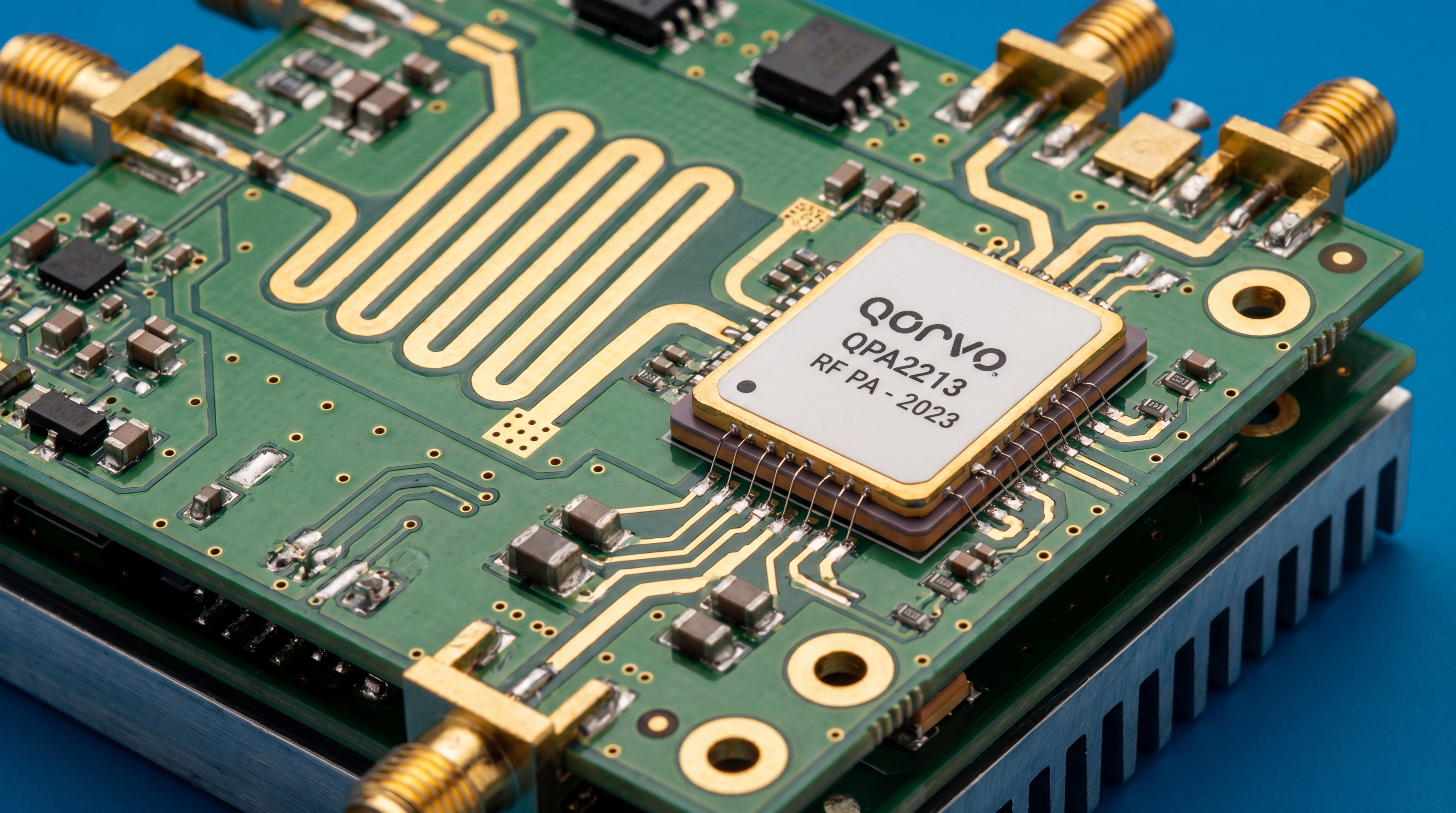
The placement of bypass capacitors is essential for an RF Power Amplifier to remain stable and noise-free. These components act as local energy reservoirs, providing quick bursts of current that the main supply cannot deliver instantly. Without them, the circuit would experience significant voltage sag during high-power pulses.
Inductive loop minimization?
The trace between the capacitor and the power pin should be as short as possible.
Here is the thing.
- Short traces reduce mounting inductance.
- Lower inductance expands effective frequency range.
- Proximity directly impacts decoupling efficiency.
Pin assignment strategies?
Each power pin on a chip should ideally have its own dedicated bypass capacitor.
This prevents noise entry.
- Small capacitors should be closest to pins.
- Dedicated caps shunt noise to ground faster.
- Multiple values provide wideband decoupling support.
Key Takeaway: Minimizing the physical distance between the capacitor and the load is the most effective way to decouple high-frequency noise.
| Cap Type | Frequency Range | Placement Priority |
|---|---|---|
| 10 pF | Microwave | Immediate proximity to pin |
| 0.1 uF | High Frequency | Within 2mm of the pin |
| 10 uF | Low Frequency | General bulk decoupling |
When should you use coplanar waveguides?
A coplanar waveguide is a powerful tool for integrating an RF Power Amplifier into a dense layout. By placing ground pours on the same layer as the signal trace, designers can achieve better isolation and control. This technique is useful when reference planes are distant or unavailable.
High-density interconnects?
In modern HDI designs, space is at a premium and layers are often very thin.
Coplanar waveguides save space.
- Lateral ground pours allow for narrower traces.
- Waveguides reduce dependence on thin dielectrics.
- Narrow traces simplify routing to fine-pitch pins.
Managing via transitions?
When a signal must move between layers, a coplanar transition helps maintain impedance.
It gets better.
- Surrounding metal guides signals through vias.
- Transitions reduce the inductive choke effect.
- Engineered transitions prevent signal bottlenecks.
Key Takeaway: Coplanar waveguides offer superior isolation and flexibility in complex, multi-layer board designs.
| Feature | Coplanar Advantage | Traditional Microstrip |
|---|---|---|
| Isolation | High (lateral ground) | Moderate |
| Trace Width | Narrower for same Z0 | Wider |
| Sensitivity | Lower to plane distance | Higher |
How do shielding and isolation reduce noise?
Effective shielding ensures that an RF Power Amplifier does not interfere with other sensitive circuits on the same PCB. This is true in compact devices where the “Internet of Analog Things” creates a crowded environment. Isolation prevents “crosstalk,” where one signal bleeds into another.
Internal shielding methods?
Shielding cans are often used to enclose high-gain blocks and prevent radiation.
Let’s dive in.
- Shielding cans block radiated EMI.
- Vias create a “Faraday cage” effect.
- Metal barriers prevent internal signal leakage.
Component grouping?
Grouping analog and digital components into separate zones is the first step toward isolation.
Separation is key.
- Physical distance reduces digital switching noise.
- Separate zones prevent signal coupling.
- Strategic placement isolates noisy power stages.
Key Takeaway: Physical separation and metal barriers are the most reliable methods for controlling electromagnetic interference.
| Method | Benefit | Implementation |
|---|---|---|
| Shielding Cans | Blocks radiated EMI | Solder over sensitive RF blocks |
| Via Fencing | Prevents lateral leakage | Staggered rows of ground vias |
| Moat Isolation | Breaks ground noise | Physical gap in the plane |
What role does dielectric material play?
Choosing the right substrate for an RF Power Amplifier is a critical decision that affects every part of the layout. The dielectric material governs how fast the signal travels and how much energy is lost. At microwave frequencies, standard materials can no longer provide necessary stability.
Dielectric constant stability?
The dielectric constant should remain stable across the entire operating temperature and frequency range.
Consistency matters.
- Stable Dk prevents impedance shifts.
- Precision hardware requires engineered laminates.
- Temperature shifts impact line characteristics.
Mitigating signal loss?
Loss tangent defines how much signal energy is absorbed by the board material itself.
Think about it.
- High-loss materials generate waste heat.
- Reduced loss increases overall system efficiency.
- Low-loss tangents ensure maximum antenna delivery.
Key Takeaway: High-performance laminates are essential for maintaining gain and efficiency in high-frequency RF systems.
| Material | Loss Tangent | Typical Use Case |
|---|---|---|
| FR4 | High | Low frequency, low cost |
| Rogers | Low | High frequency, precision RF |
| PTFE | Very Low | Millimeter-wave, high power |
How do vias affect high-frequency signals?
Vias are often the weakest link in the signal path of an RF Power Amplifier. A standard through-hole via acts as a parasitic inductor and capacitor, creating a massive impedance mismatch. Managing these transitions is essential for maintaining a clean signal from input to output.
Managing impedance mismatch?
A via’s geometry should be tuned to match the 50-ohm impedance of the connecting traces.
Here is the thing.
- Larger anti-pads reduce parasitic capacitance.
- Ground stitching vias surround signal paths.
- Proper tuning prevents signal reflections.
Air gap optimization?
The air gap around a signal via determines its capacitance to surrounding ground planes.
It gets better.
- Optimized gaps cancel out natural inductance.
- Flat impedance profiles ensure signal purity.
- Precision gaps minimize transition bottlenecks.
Key Takeaway: Every layer transition must be carefully engineered to prevent it from acting as a signal bottleneck.
| Via Type | Frequency Limit | Design Consideration |
|---|---|---|
| Through-Hole | ~5 GHz | Tuning and ground stitching |
| Blind/Buried | ~20 GHz | Reduced parasitic stubs |
| Microvia | >40 GHz | Smallest parasitic impact |
Can layout techniques improve heat management?
Heat is the enemy of any high-output RF Power Amplifier, causing performance drift and reducing component lifespan. Effective thermal management starts with the layout, ensuring heat is drawn away from active silicon. Copper is the most efficient tool for this task.
Thermal via implementation?
Placing a dense array of vias under the amplifier’s pad creates a low-resistance thermal path.
This is efficient.
- Thermal vias conduct heat to ground planes.
- Low-resistance paths prevent silicon overheating.
- Effective cooling extends hardware lifespan.
Copper pour strategies?
Large copper pours on the outer layers act as heat sinks, dissipating energy into the air.
Let’s dive in.
- Large surface areas improve convection cooling.
- Internal connections maximize thermal mass.
- Proactive layout prevents thermal gain drift.
Key Takeaway: Proactive thermal layout prevents hardware failure and ensures consistent performance under heavy duty cycles.
| Thermal Tool | Cooling Method | Key Requirement |
|---|---|---|
| Thermal Vias | Conduction | Direct path to massive planes |
| Copper Pours | Convection | Large surface area exposure |
| Heat Sinks | External Dissipation | Low-impedance interface |
To ensure your high-frequency design succeeds, you must integrate these transmission line and PDN principles. For professional support or to discuss your specific engineering requirements, please contact us.
FAQ
How can I determine the correct trace width for 50 ohms?
You should use a specialized impedance calculator that accounts for your specific dielectric height, material constant, and copper weight.
Can I use FR4 for RF layouts under 2 GHz?
Yes, FR4 is typically sufficient for lower frequencies if you account for its higher loss tangent and wider manufacturing tolerances.
How do I know if my PDN is causing noise in my RF signal?
You can identify PDN-related noise by observing spectral regrowth or jitter that correlates with current spikes in your power supply.
Can I place a ground plane directly under my printed antenna?
Generally, you should clear ground planes directly under the antenna to allow it to radiate, though surrounding areas should be heavily stitched.
What is the best way to transition RF signals between layers?
The most effective method is using a tuned via transition surrounded by a cage of ground stitching vias to maintain impedance and shielding.