
Broadband solid-state efficiency, thermal optimization, and high-frequency monolithic integration are the core updates shaping modern GaN for RF technology today. High-speed wireless infrastructure, satellite communication, and advanced defense systems are hitting a hard physical bottleneck because legacy RF semiconductors, such as Silicon (Si) and Gallium Arsenide (GaAs), cannot handle the simultaneous demands of ultra-high frequency, massive output power, and compact thermal footprints required by modern RF architectures. Engineers are forced to choose between bulky, fragile traveling wave tubes or complex power-combining networks of inefficient GaAs amplifiers, leading to massive thermal dissipation issues, reduced system reliability, increased payload weights, and soaring development budgets. Fortunately, solid-state wide-bandgap technology has stepped in to rewrite the rules and solve these persistent high-power RF system pain points. This article outlines the latest advancements in GaN for RF Technology, demonstrating how optimized micro-assembly and chip design enable unprecedented power density and frequency coverage from HF through millimeter-wave bands.
What is GaN and how is it used in RF systems?
Gallium Nitride (GaN) is a high-electron-mobility, wide-bandgap semiconductor that serves as the premier channel material for high-power, high-frequency RF components. The integration of GaN for RF Technology has revolutionized modern high-power solid-state amplifiers. Its wide bandgap of 3.4 eV allows devices to operate at significantly higher voltages, improving ruggedness and simplifying impedance-matching networks across massive operating bandwidths. You can now achieve unparalleled transmission ranges while drastically reducing your system’s overall footprint.
Why does GaN outperform traditional GaAs?
When you analyze the electrical properties that govern performance, you quickly realize why legacy devices struggle. GaAs has long been the standard for low-noise and medium-power applications, but its low breakdown voltage limits its physical power-handling capacity.
Here is why this matters:
- Higher Breakdown Voltage: Allows your systems to operate at 28V, 48V, or higher.
- Superior Power Density: Delivers up to 5 to 10 times the power per millimeter of gate width.
- Excellent Thermal Thresholds: Operates safely at channel temperatures exceeding 200°C without rapid degradation.
Which RF components are now using GaN?
If your RF front end is bottlenecked by fragile switches and lossy mixers, your high-power amplifier gains are wasted. Consequently, modern system integration relies on GaN far beyond simple power amplification blocks to protect signal integrity.
But wait, there is more:
- Low-Noise Amplifiers (LNAs): Achieves high dynamic range and robust receiver protection.
- Robust Limiters: Prevents receiver burnout from high-power co-site signals.
- High-Isolation Switches: Directs signal routing with minimal insertion loss.
Key Takeaway
GaN is transitioning your RF design from hybrid multi-technology modules to unified, highly rugged, solid-state wideband architectures.
Let us evaluate the core physical properties of these key semiconductor technologies:
| Parameter | Silicon (Si) | Gallium Arsenide (GaAs) | Gallium Nitride (GaN) |
|---|---|---|---|
| Bandgap Energy (eV) | 1.12 | 1.43 | 3.40 |
| Breakdown Field (MV/cm) | 0.3 | 0.4 | 3.3 |
| Electron Mobility (cm²/V·s) | 1500 | 8500 | 1500–2000 |
| Saturated Drift Velocity (10⁷ cm/s) | 1.0 | 1.0 | 2.5 |
The clear superiority of GaN across bandgap energy and breakdown field underpins its modern dominance in the RF domain.
How do different GaN substrates compare in RF?
The choice of substrate material—predominantly Silicon Carbide (SiC) or Silicon (Si)—dictates the thermal performance, maximum frequency, and cost-efficiency of the RF device. When evaluating GaN for RF Technology, you must match the underlying substrate with your specific application parameters. Substrate thermal conductivity acts as the ultimate gatekeeper of performance, determining whether a device can maintain peak output power under continuous-wave conditions.
What are the benefits of GaN on SiC?
GaN-on-SiC is the undisputed gold standard for high-reliability, high-power RF applications. Silicon carbide possesses a thermal conductivity that closely matches the extreme power dissipation of GaN channels, preventing the formation of catastrophic localized hot spots.
Here is why this matters:
- Extreme Thermal Conductivity: SiC offers ~120% higher thermal performance than silicon substrates.
- Reduced Lattice Mismatch: Lowers dislocation density at the epitaxial boundary, improving device lifespan.
- Lower Parasitic Capacitance: Enhances high-frequency efficiency and gain flatness up to millimeter-wave regions.
When is GaN on silicon more practical?
While SiC dominates high-end military and aerospace programs, commercial scalability demands a different approach. GaN-on-Si utilizes cheap, existing silicon semiconductor manufacturing lines, dramatically reducing unit costs.
But wait, there is more:
- Mass-Market Scalability: Ideal for commercial cellular base stations.
- Sub-6 GHz Focus: Highly optimized for standard commercial telecom bands.
- Lower Initial Investment: Fits tight commercial prototyping budgets.
Key Takeaway
Choose GaN-on-SiC for high-frequency, high-power density military and SATCOM systems, and GaN-on-Si for high-volume, cost-constrained sub-6 GHz networks.
Let us review the key substrate parameters and application targets:
| Substrate Material | Thermal Conductivity (W/m·K) | Relative Wafer Cost | Target Frequency Range | Typical Applications |
|---|---|---|---|---|
| Silicon (Si) | ~150 | Low | DC to 10 GHz | Mass-market 5G, consumer RF |
| Silicon Carbide (SiC) | ~350–450 | High | DC to 100 GHz | Defense, Radar, SATCOM Ground |
| Diamond | >2000 | Extremely High | 10 GHz to THz | Experimental MMICs, Deep Space |
Understanding substrate tradeoffs is critical to selecting the correct platform for your thermal environment.
Why is GaN replacing LDMOS in high-power RF?
GaN has surpassed LDMOS because it delivers substantially higher power-added efficiency (PAE) and wider bandwidths at operating frequencies above 2 GHz. Integrating modern GaN for RF Technology resolves physical limitations, allowing you to consolidate multiple narrowband LDMOS modules into a single wideband platform. This efficiency transition simplifies your power-combining architectures and reduces your cooling costs.
How does GaN improve power density?
Silicon-based LDMOS is physically limited by its low breakdown voltage and high parasitic capacitances. GaN’s wide bandgap enables higher drain voltage operation, which dramatically shrinks the required die size for a given output power.
Here is why this matters:
- Miniaturized Footprints: Reduces power amplifier module volume by up to 70%.
- Simplified Matching: High drain impedance makes broadband matching networks easier to design.
- Decreased Weight: Slashes payload weight for airborne platforms and mobile defense rigs.
What efficiency gains do PAs achieve?
Thermal waste is the primary failure driver in remote, tower-mounted, or enclosed RF environments. Let’s face it, an inefficient amplifier is merely an expensive heater that incidentally transmits RF.
But wait, there is more:
- Higher PAE Levels: Routinely delivers PAE levels 15% to 25% higher than LDMOS.
- Reduced Thermal Load: Direct decrease in system operating temperatures.
- Lower Operating Costs: Slashes power supply demands over the lifecycle.
Key Takeaway
GaN renders LDMOS obsolete above 2 GHz by offering higher operating voltages, broader bandwidths, and superior operational efficiency.
Let us compare LDMOS with GaN across key metrics:
| Metric | LDMOS (Silicon) | GaN (on SiC) | System-Level Impact |
|---|---|---|---|
| Typical Operating Voltage | 28V–32V | 48V–50V | Lower current draw, simplified power supply |
| Max Frequency Limit | ~3.5 GHz | >100 GHz | Opens Ka-band and millimeter-wave designs |
| Typical PAE at 3.5 GHz | 30%–38% | 55%–70% | Drastically reduced heat sink size |
| Saturated Power Density | <1.5 W/mm | 5–20 W/mm | Smaller physical die sizes, tighter integration |
The operational shift from LDMOS to GaN provides immediate system-level benefits in efficiency and size.
Can GaN technology replace high-frequency TWTAs?
Yes, GaN solid-state power amplifiers (SSPAs) are systematically replacing Traveling Wave Tube Amplifiers (TWTAs) in defense and satellite applications due to their superior reliability and graceful degradation characteristics. Utilizing GaN for RF Technology allows you to implement spatial power combining to build highly reliable, solid-state transmitters that run on safe, low-voltage DC rails. This transition eliminates high-voltage power supply hazards from your installations.
Is solid-state GaN ready for SATCOM?
Space-borne and satellite ground-terminal environments demand flawless operation over decades. TWTAs suffer from high wear-and-tear mechanisms, requiring high-voltage power supplies exceeding 10 kV that are prone to catastrophic failure.
Here is why this matters:
- Graceful Degradation: Parallel combining allows system operation to continue even if one transistor fails.
- Low-Voltage Operation: Runs on standard 48V DC systems, removing high-voltage arcing risks.
- Zero Warm-Up Time: Provides instantaneous power transmission when you need it.
How does GaN perform in Ka-band systems?
High-frequency SATCOM relies on wider spectral blocks to maximize data throughput. GaN SSPAs not only match TWTA power levels at Ka-band, but they also offer superior phase noise performance and higher linearity under multi-carrier operations.
But wait, there is more:
- Higher Modulation Schemes: Supports 64-APSK with minimal error vector magnitude (EVM).
- Superior Signal Quality: Delivers clean, undistorted paths for dense data.
- Improved Thermal Stability: Maintains performance across orbital temperature swings.
Key Takeaway
GaN SSPAs have matured to replace TWTAs up to Ka-band, offering dramatic increases in operational reliability, signal quality, and mission lifespans.
Let us compare the capabilities of TWTAs and GaN SSPAs:
| Parameter | Traveling Wave Tube (TWTA) | GaN Solid-State (SSPA) |
|---|---|---|
| Operating Voltage | 3 kV to >10 kV (High-voltage risk) | 28V to 50V DC (Safe, low voltage) |
| Failure Mode | Catastrophic (Single-point filament burn-out) | Graceful (Individual transistor degradation) |
| Warm-Up Delay | 3 to 5 minutes | Instantaneous (<1 microsecond) |
| Physical Ruggedness | Low (Fragile glass/ceramic vacuum tubes) | High (Monolithic semiconductor on SiC) |
SSPA technology eliminates the single point of failure and high voltage hazards inherent in vacuum tubes.
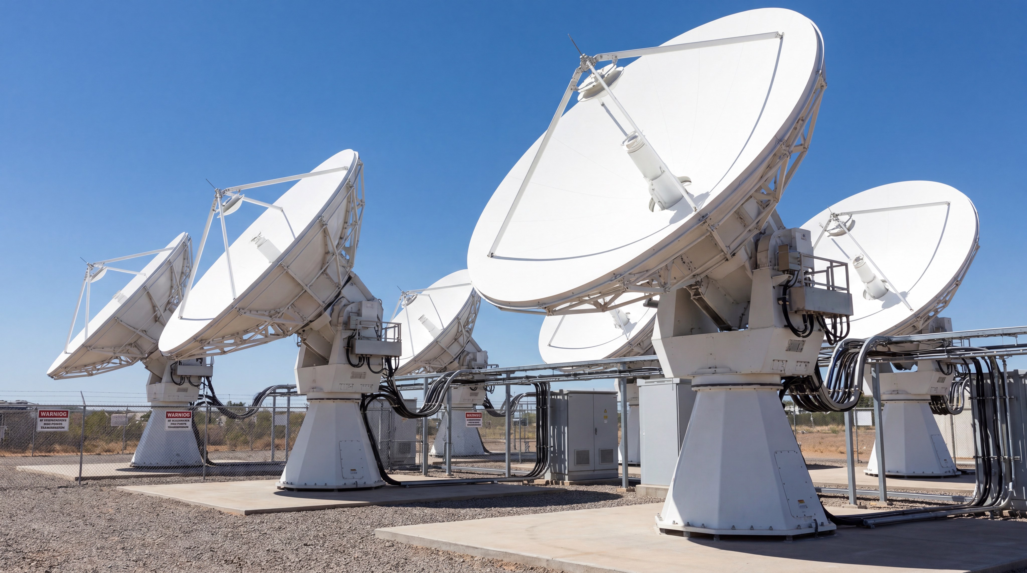
Ground Station Antenna Arrays
What role does GaN play in modern 5G networks?
GaN is the primary enabler of 5G infrastructure, delivering the high output power and linearity required to drive massive MIMO (m-MIMO) active antenna arrays. Incorporating GaN for RF Technology allows telecom manufacturers to fit high-efficiency, multi-watt amplifiers into the tight physical spacing dictated by antenna pitch. This dense integration is essential for modern beamforming arrays.
How does GaN support sub-6 GHz MIMO?
Sub-6 GHz networks require massive bandwidths and high-power density to maintain coverage in dense urban environments. GaN’s wide fractional bandwidth simplifies hardware deployment by covering multiple telecom bands with a single amplifier.
Here is why this matters:
- No Active Fans: High thermal efficiency eliminates cooling fans, reducing operator utility and maintenance costs.
- Excellent Linear Power: Maintains high efficiency under high peak-to-average power ratio (PAPR) OFDM signals.
- Unified Architectures: Replaces complex multi-chip legacy solutions easily.
Can GaN handle 5G millimeter-wave?
Millimeter-wave frequencies demand incredibly high power from compact arrays to overcome high atmospheric propagation losses. GaN MMICs integrate the power amplifier, LNA, and switch on a single die, minimizing routing losses.
But wait, there is more:
- Maximum EIRP: Achieves peak effective isotropic radiated power from compact arrays.
- Miniaturized Front-Ends: Fits directly behind individual antenna elements.
- Scalable Architecture: Simplifies array expansions for dense urban deployments.
Key Takeaway
GaN is the only semiconductor technology capable of meeting the simultaneous power, thermal, and frequency requirements of high-density 5G base stations.
Let us review 5G band requirements and semiconductor choices:
| 5G Band Category | Frequency Range | Primary Competitor | GaN Advantage |
|---|---|---|---|
| Sub-6 GHz (MIMO) | 3.3 GHz – 4.9 GHz | LDMOS / GaAs | High PAE at high peak-to-average power ratios |
| FR2 mmWave (Beamforming) | 24 GHz – 40 GHz | Silicon RFSOI / SiGe | Higher EIRP per element, overcoming path loss |
| Advanced mmWave Backhaul | 71 GHz – 86 GHz | GaAs / InP | Higher output power to extend point-to-point distance |
The exceptional power density of GaN makes it indispensable for millimeter-wave backhaul links.
How does GaN improve pulse radar performance?
GaN dramatically improves pulse radar systems by enabling exceptionally high peak output power and fast rise/fall times within compact aperture arrays. Utilizing GaN for RF Technology delivers high peak power density, enabling radars to detect smaller targets at much longer ranges. Modern active electronically scanned array (AESA) radars benefit immensely from this rapid signal response.
Why is GaN ideal for defense jamming?
Electronic warfare (EW) and defense jamming systems must sweep across massive frequency bands instantaneously to overpower hostile threats. A single GaN amplifier can cover multi-octave ranges, replacing banks of legacy devices.
Here is why this matters:
- Broadband Coverage: A single amplifier can cover multi-octave ranges, replacing legacy bands.
- High Survivability: GaN’s high breakdown voltage survives severe antenna mismatch (VSWR) conditions.
- Clean Modulation: Delivers clean, high-speed pulse modulation with minimal distortion or phase jitter.
How do pulsed GaN PAs maximize peak power?
Thermal management in pulsed radar relies on the short duty cycle of the signal. Because the RF pulse is active for only a fraction of the time, pulsed GaN amplifiers can be driven into deep saturation during the “on” cycle.
But wait, there is more:
- High Saturation Limits: Safely outputs tens of kilowatts of peak power.
- Fast Thermal Relief: Allows rapid cooling of the channel during the “off” cycle.
- Extended Range: Increases target detection distance on search radars.
Key Takeaway
GaN transforms radar design by enabling solid-state AESA arrays to match the peak range capabilities of legacy magnetron and klystron systems.
Let us analyze pulsed radar performance comparisons:
| Pulse Radar Parameter | GaAs Capability | GaN Capability | System Capability Impact |
|---|---|---|---|
| Peak Power per T/R Module | ~5W to 15W | >100W to 500W | Up to 10x increase in target detection range |
| VSWR Ruggedness | Sensitive to reflection | Survives up to 10:1 VSWR | Operational survival during antenna damage |
| Duty Cycle Capability | Limited by thermal lag | Up to 50% duty cycle | Supports highly complex, dense radar waveforms |
The massive upgrade in peak power per module translates directly to broader defense coverage.
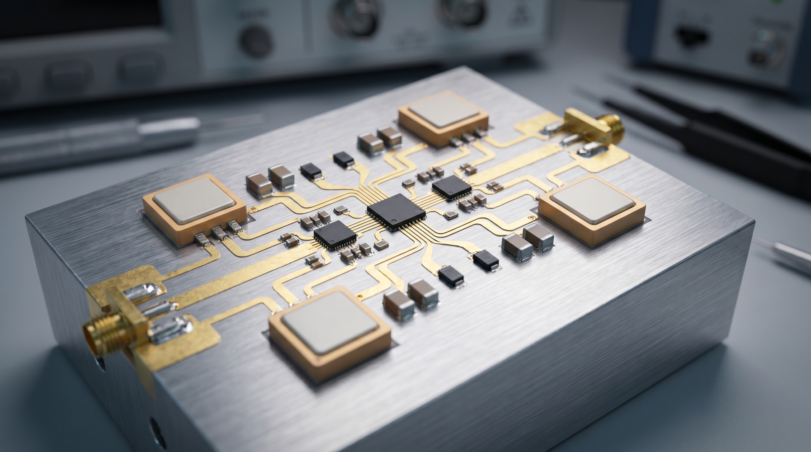
Advanced RF Packaging Lab
What are the thermal challenges in GaN RF design?
Although GaN can withstand high junction temperatures, its extreme power density generates localized micron-scale “hot spots” that require highly engineered thermal extraction paths. While GaN for RF Technology offers unrivaled electrical performance, placing tens of watts of power inside a sub-millimeter transistor channel creates extreme heat flux. Failing to evacuate this heat causes junction temperatures to exceed safe operational limits.
Why is thermal management critical?
The reliability of your semiconductor is exponentially dependent on its junction temperature. If the local channel temperature is allowed to spike, the device’s electron mobility drops, leading to a permanent drop in output power and gain.
Here is why this matters:
- Hot Spot Mitigation: Transistor gates can generate heat flux densities comparable to the surface of the sun.
- Thermal Expansion Matching: Mismatched expansion coefficients lead to mechanical cracking.
- CW Performance: Uncontrolled thermal resistance restricts continuous-wave operation.
Can GaN on diamond solve heat issues?
To bypass the limitations of silicon and silicon carbide, researchers are turning to ultimate-thermal materials. By bonding GaN epitaxial layers directly to synthetic chemical vapor deposition (CVD) diamond substrates, you can utilize a material with superior properties.
But wait, there is more:
- Fourfold Thermal Improvement: Diamond offers thermal conductivity four times greater than SiC.
- Higher Drive Currents: Transistors can be driven up to three times harder.
- Reduced Mechanical Stress: Lowers overall expansion mismatches across the assembly.
Key Takeaway
Packaging is the primary bottleneck in GaN RF design; utilizing advanced thermal substrates like CVD diamond is essential to unlocking the material’s true electrical potential.
Let us evaluate standard thermal materials used in RF packaging:
| Thermal Material | Thermal Conductivity (W/m·K) | CTE (10⁻⁶/K) | Integration Complexity |
|---|---|---|---|
| Copper (Cu) | 400 | 16.5 | Low (Standard heat sinks) |
| Silicon Carbide (SiC) | 400 | 4.0 | Medium (Industry-standard GaN carriers) |
| Copper-Tungsten (CuW) | 180–220 | 5.6–8.3 | Medium (Excellent CTE match to ceramics) |
| CVD Diamond | 1200–2000 | 1.1–1.5 | Extremely High (Experimental bonding) |
Selecting the right thermal interface and packaging materials avoids localized hot spot failures.
Is GaN reliable enough for aerospace and space?
Yes, GaN has proven highly reliable for harsh aerospace and space applications due to its inherent radiation hardness and exceptional physical ruggedness. Space-bound equipment must survive extreme G-forces during launch, operate in vacuum conditions, and withstand constant bombardment from cosmic radiation, which makes GaN for RF Technology the ideal choice. Its wide bandgap structure makes it naturally resistant to Single Event Effects (SEE) and Total Ionizing Dose (TID) degradation.
How rugged is GaN in harsh environments?
Military and space-grade systems operate far beyond the stable thermal zones of commercial laboratories. When you deploy in these domains, your hardware must resist physical shocks, cosmic radiation, and sudden thermal shifts.
Here is why this matters:
- Radiation Hardness: Wide bandgap material is highly immune to lattice displacement caused by cosmic protons.
- Extreme Operating Ranges: Devices operate reliably from cryogenic temperatures up to +225°C.
- High Voltage Immunity: High dielectric breakdown strength prevents gate puncture during transient strikes.
What is the typical lifespan of a GaN PA?
Space missions are designed for multi-decade, zero-maintenance lifespans to ensure uninterrupted connectivity. Rigorous High-Temperature Operating Life (HTOL) testing shows that properly packaged GaN-on-SiC devices exhibit exceptional lifespans.
But wait, there is more:
- Million-Hour MTTF: Exceeds 1 million hours at junction temperatures of 200°C.
- Zero Drift Profiles: Maintains consistent gain levels over long-term operations.
- Zero Moisture Ingress: Achieved through advanced hermetic sealing techniques.
Key Takeaway
GaN’s high physical breakdown limits and resistance to radiation make it the premier choice for deep-space communication and military aerospace payloads.
Let us review key space qualification metrics and performance:
| Qualification Test | Standard Target | GaN Performance | Mission Advantage |
|---|---|---|---|
| Total Ionizing Dose (TID) | >100 krad | Survives >1 Mrad | Extended lifespan in high-radiation orbits |
| Single Event Burnout (SEB) | No latch-up | Immune up to high LET | Eliminates latch-up protection circuitry |
| HTOL Lifetime | 1,000 hours at rated temp | MTTF > 10⁶ hours at 200°C channel temp | Zero-maintenance operation for 15+ year satellites |
These reliable physical thresholds make GaN the preferred technology for orbit payloads.
What are the current market trends for RF GaN?
The RF GaN market is experiencing rapid expansion, fueled by defense modernization, SATCOM commercialization, and global 5G millimeter-wave rollouts. The market landscape for GaN for RF Technology is transitioning from low-volume military niches to high-volume commercial manufacturing. This shift has driven massive foundry investments, leading to improved wafer yields, standardized testing protocols, and lower barrier-to-entry costs.
What is the projected CAGR for GaN?
Market analyst firms consistently place GaN among the fastest-growing sectors in the RF semiconductor landscape. As production processes mature, you will witness dramatic price drops and greater commercial accessibility.
Here is why this matters:
- Double-Digit Annual Growth: Projected compound annual growth rate (CAGR) exceeds 12% through 2030.
- Commercial Shift: Commercial telecom infrastructure is expected to surpass defense spending as the largest revenue driver.
- Wafer Optimization: Transitioning from 4-inch to 6-inch and 8-inch wafer lines reduces unit prices.
Which industries drive the highest demand?
While defense remains the foundational baseline, civilian applications are scaling rapidly. Modern consumers demand infinite data bandwidth, and defense forces require complete spectrum dominance.
But wait, there is more:
- SATCOM Ground Terminals: Massive growth in LEO satellite gateways.
- UAV Communications: High-power, lightweight datalinks.
- Smart Radars: Standardized AESA units for commercial maritime navigation.
Key Takeaway
The RF GaN market is accelerating quickly, with commercial 5G/6G infrastructure and LEO satellite megaconstellations representing the primary growth engines.
Let us summarize the core market drivers across segments:
| Market Segment | Primary Hardware Driver | Growth Outlook (Through 2030) | Main Performance Metric Demanded |
|---|---|---|---|
| Defense / EW | AESA Radar, wideband jammer arrays | Steady (8-10% CAGR) | Maximum peak power, VSWR ruggedness |
| Commercial Telecom | 5G/6G massive MIMO base stations | High (12-15% CAGR) | Power-added efficiency (PAE), low unit cost |
| SATCOM (LEO) | LEO satellite terminals, gateway SSPAs | Exponential (>20% CAGR) | Ka-band efficiency, compact payload footprint |
High foundry investments ensure a secure global supply chain for B2B procurement.
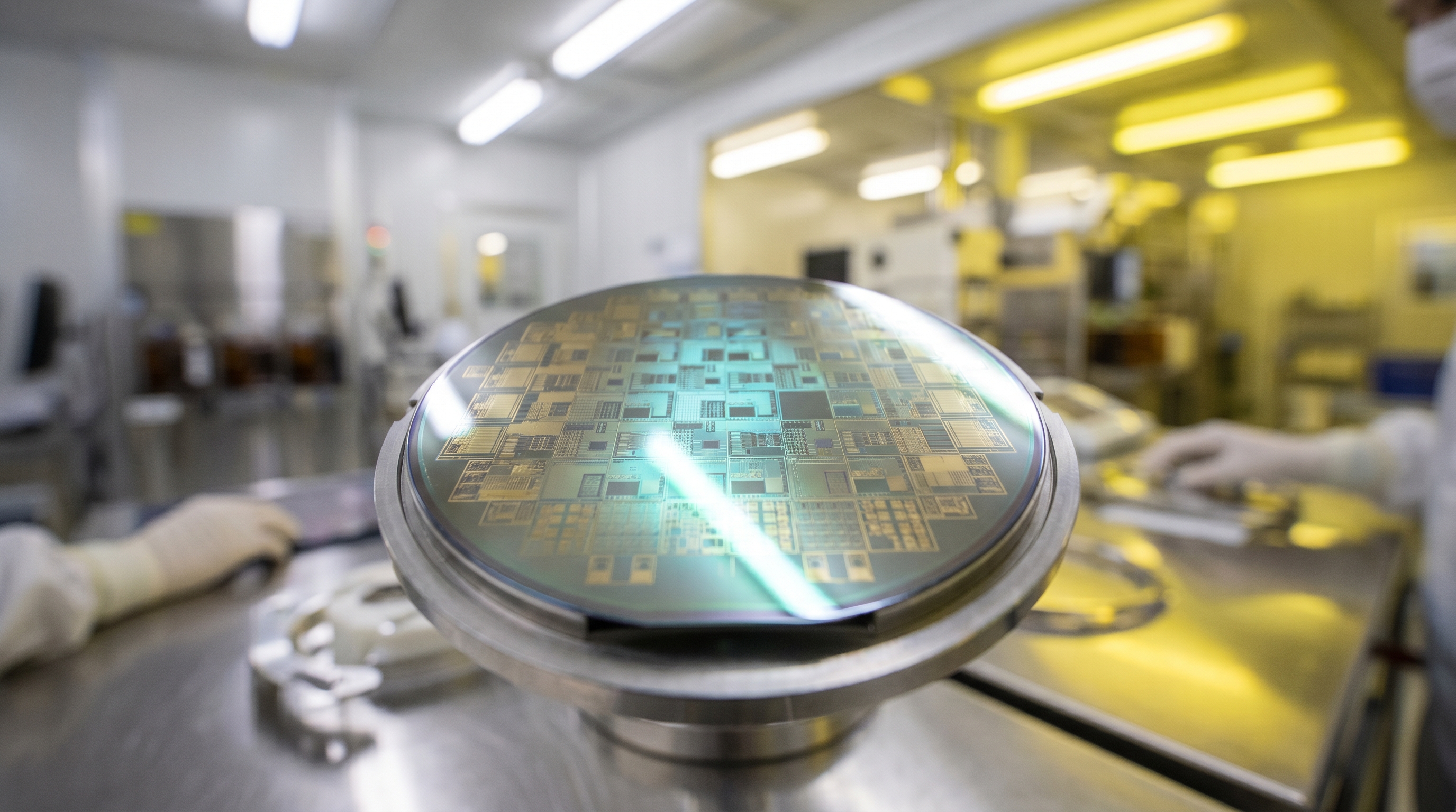
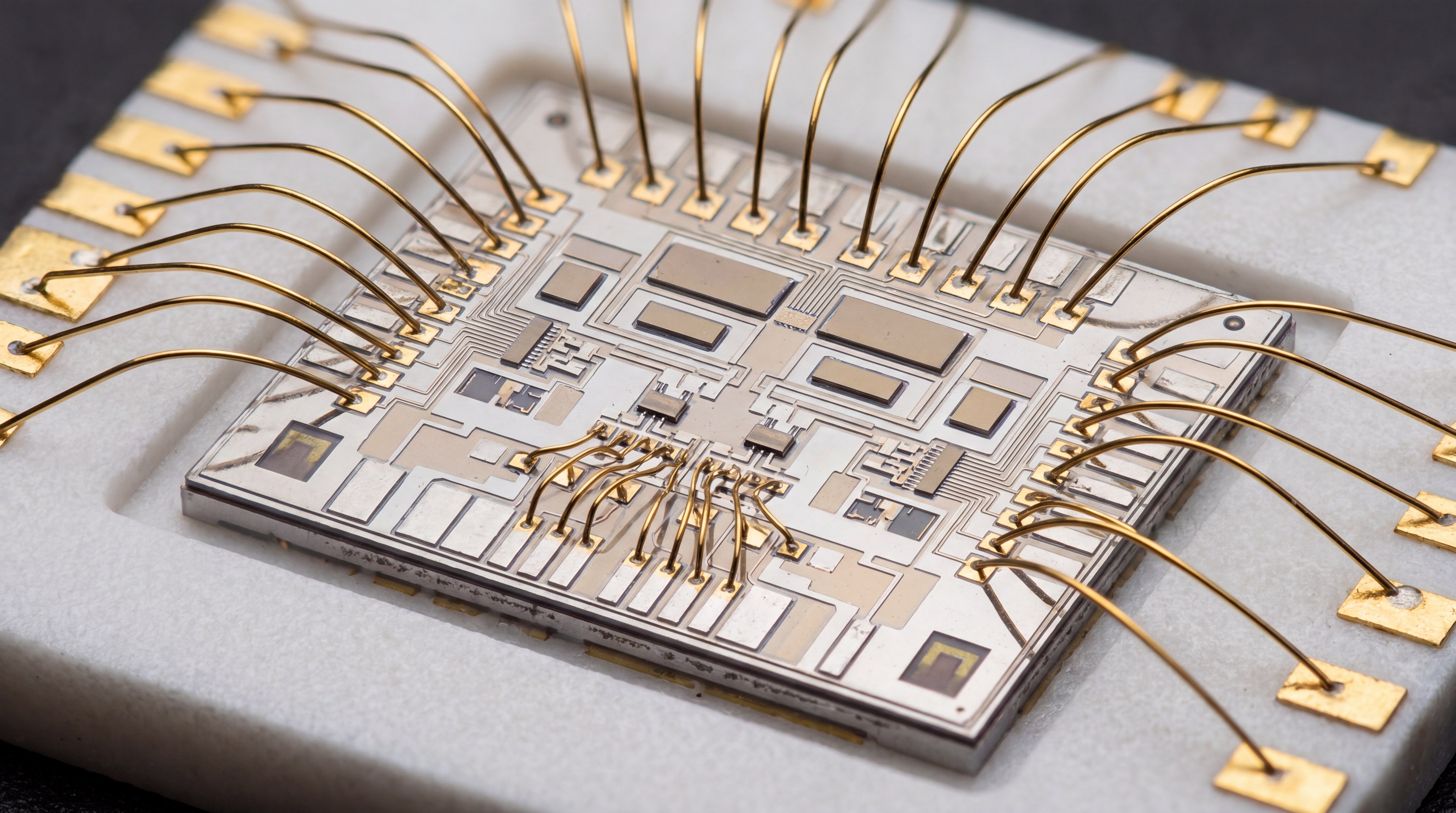
Advanced GaN Processing and Quality Control
What does the future hold for GaN RF devices?
The future of GaN lies in monolithic sub-system integration, terahertz operating limits, and hybrid multi-material packaging that maximizes thermal dissipation. As we look beyond current limits, GaN for RF Technology is pushing into the sub-millimeter-wave and terahertz zones. These next-generation steps will enable ultra-secure, ultra-high-bandwidth point-to-point communications and ultra-high-resolution imaging radars.
Can GaN operate at terahertz frequencies?
Standard high-frequency devices typically roll off as they approach 100 GHz. However, recent R&D has successfully fabricated GaN HEMTs with gate lengths scaled down to sub-50 nanometers.
Here is why this matters:
- Sub-50nm Gates: Enables ultra-short channels for high cutoff frequencies ($f_T$) exceeding 300 GHz.
- Terabit-per-Second Backhaul: Supports extreme bandwidth communications.
- Millimeter-Wave Security Scanning: Enables ultra-fine resolution scanning.
What R&D breakthroughs are on the horizon?
The next evolutionary leap will focus on material convergence. Research into heterogeneous integration allows GaN dies to be directly bonded onto silicon CMOS control wafers at the wafer level.
But wait, there is more:
- Monolithic Logic: Integrates high-power GaN output with ultra-dense silicon logic.
- Intelligent Bias Schemes: Optimizes power dynamically on a single chip.
- Parasitic Reduction: Removes bond wire losses for improved efficiency.
Key Takeaway
The future of GaN will redefine system architecture by combining terahertz frequency limits with intelligent, monolithic logic integration.
Let us compare current boundaries with future targets:
| Development Metric | Current Generation GaN | Next-Generation GaN Target | Enabling R&D Technology |
|---|---|---|---|
| Max Frequency ($f_T$) | ~100 GHz | >300 GHz | Sub-50nm gate scaling, improved barrier layers |
| Thermal Substrate | Silicon Carbide (SiC) | Diamond / AlN | Direct wafer-level bonding to CVD diamond |
| System Integration | Discrete / Hybrid MMIC | Heterogeneous Monolithic | Direct integration of GaN RF with Silicon CMOS |
R&D advancements are quickly bridging the gap between millimeter-wave power limits and sub-terahertz logic.
Conclusion
By addressing the classic trade-offs of power, frequency, and thermal stability, the evolution of GaN has fundamentally transformed the RF engineering landscape. It has rendered legacy LDMOS obsolete above 2 GHz and is successfully replacing high-voltage TWTAs in critical SATCOM and defense environments.
When integrating GaN hardware, procurement and engineering teams must look beyond raw datasheet numbers. It is vital to partner with a manufacturer that controls the complete engineering chain—from chip design and precision micro-assembly to unit-level active testing and ISO 9001/GJB 9001C validation.
Ready to migrate your high-power or high-frequency RF project to solid-state GaN? Whether you need standard broadband modules, Ka-band SATCOM amplifiers, or custom OEM/ODM solutions, contact us today to collaborate directly with our factory-direct engineering team and receive a complete feasibility review within 24 to 48 hours. Our mission is to empower global engineering teams with rugged, high-performance solid-state platforms that expand the boundaries of modern connectivity.
Technical FAQ
Can I integrate GaN power amplifiers into my existing LDMOS or GaAs setups?
Yes, absolutely. However, you must carefully evaluate your bias sequence and operating voltages. GaN HEMTs are depletion-mode devices that require a negative gate voltage to be applied before the positive drain voltage to prevent catastrophic current spikes. Additionally, GaN runs at higher voltages (28V–50V) compared to GaAs (5V–12V), requiring power supply redesigns.
What’s the best way to choose between GaN-on-SiC and GaN-on-Si for my design?
The best selection is determined by your target frequency, power density requirements, and budget limits. You should choose GaN-on-SiC if your application requires maximum power density, operates above 10 GHz, or runs continuously under extreme thermal conditions where reliability is paramount. Choose GaN-on-Si if you are designing high-volume, cost-sensitive commercial hardware below 6 GHz where silicon foundries can significantly lower unit costs.
How do I know if a standard GaN RF platform can be customized for non-standard bands?
Yes, you can easily adapt standard designs by partnering with a factory-direct manufacturer. Our in-house engineering team can tune matching networks, modify connector styles, customize mechanical housings, and adjust bias configurations to meet your precise frequency, gain flatness, and packaging constraints.
How do I know if my design is protected against thermal runaway?
You should ensure that a multi-tiered thermal extraction strategy is implemented. This includes utilizing high-conductivity base plates (such as Copper-Tungsten or Copper), optimizing the thermal interface material (TIM) between the module and the system chassis, and incorporating active temperature monitoring with automatic shutdown circuitry to protect the GaN junction if temperatures exceed 225°C.
Can I request individual unit-level test data before my equipment is shipped?
Yes, absolutely. High-reliability integration requires starting with a verified performance baseline. We do not use sampled or estimated data; every applicable GaN amplifier unit undergoes individual active testing across its entire operating band to verify output power, gain flatness, harmonics, and VSWR before it leaves our certified facility.