
Fixing RF Drive & DC Power Sequence Burnouts In Systems requires precise engineering methodology. Complex integrated systems often face unexpected hardware failures during initial testing phases. Uncoordinated activation between direct current supplies and microwave excitation signals destroys expensive modules instantly. We solve this anomaly through strict timing protocols alongside robust component selection. My two decades of troubleshooting solid-state amplifiers guarantees proven verification strategies.
Bring RF amplifier power sequencing into system-level review
Hardware interlocks and power sequencing should be reviewed with amplifier class, RF front-end timing, control interface, protection logic and FAT evidence. CorelixRF can align these before quote stage.
1. What Causes Instant Burnout In Complex Integrated Systems?
● Timing Discrepancies
Timing discrepancies represent major failure vectors inside high-power microwave systems. Engineers must understand absolute microsecond delays between individual system components. Different power supplies ramp up voltages at wildly different speeds. Relays add further unpredictable mechanical delays during activation cycles.
● Transistor Gate Stress
Transistor gate stress destroys costly semiconductor junctions within milliseconds. Unbiased gates cannot block massive current flows from main drain supplies. Localized heating melts internal gold wire bonds rapidly.
● High-Frequency Vibration Impacts
High-frequency vibration impacts degrade mechanical connections inside mobile platforms severely. Loose wiring harnesses delay gate bias delivery behind incoming continuous wave signals. System integrators must recognize these specific hardware vulnerabilities immediately.
Here is the exact deal. Unsynchronized activation sequences destroy gallium nitride transistors within microseconds. Engineers frequently apply microwave power before establishing correct gate bias voltage. This oversight causes massive drain current spikes across internal semiconductor channels. Device junctions overheat rapidly under such uncontrolled electrical stress conditions. We observe this catastrophic failure frequently inside mobile electronic warfare pods. High-frequency vibration aggravates loose power connections. Intermittent voltage drops trigger unpredictable bias state fluctuations. Radio frequency excitation entering an unbiased amplifier creates severe impedance mismatches. Reflected energy compounds thermal loading on front-end matching networks. Burnouts happen before standard over-current protection mechanisms can react. Take radar testing facilities operating multiple transmitter racks simultaneously. Technicians powering main buses before activating local control units face instantaneous module vaporization. Consider shipboard communication arrays facing heavy saltwater corrosion daily. Degraded ground planes cause erratic DC supply spikes destroying sensitive RF front ends. Look at unmanned aerial vehicle payloads enduring massive launch forces. Loose wiring harnesses delay gate bias delivery behind incoming continuous wave signals.
| Parameter | Safe Condition | Failure Condition | Consequence |
| Gate Bias | Present before RF | Absent or delayed | Transistor saturation |
| Drain Voltage | Stable 28V DC | Fluctuating transient | Thermal runaway |
| Drive Signal | Applied last | Applied first | Immediate catastrophic damage |
| Vibration Level | Dampened mounting | High-frequency shock | Intermittent connector contact |
2. How Do We Reconstruct Failure Scenes Using Oscilloscopes?
● Probing Power Lines
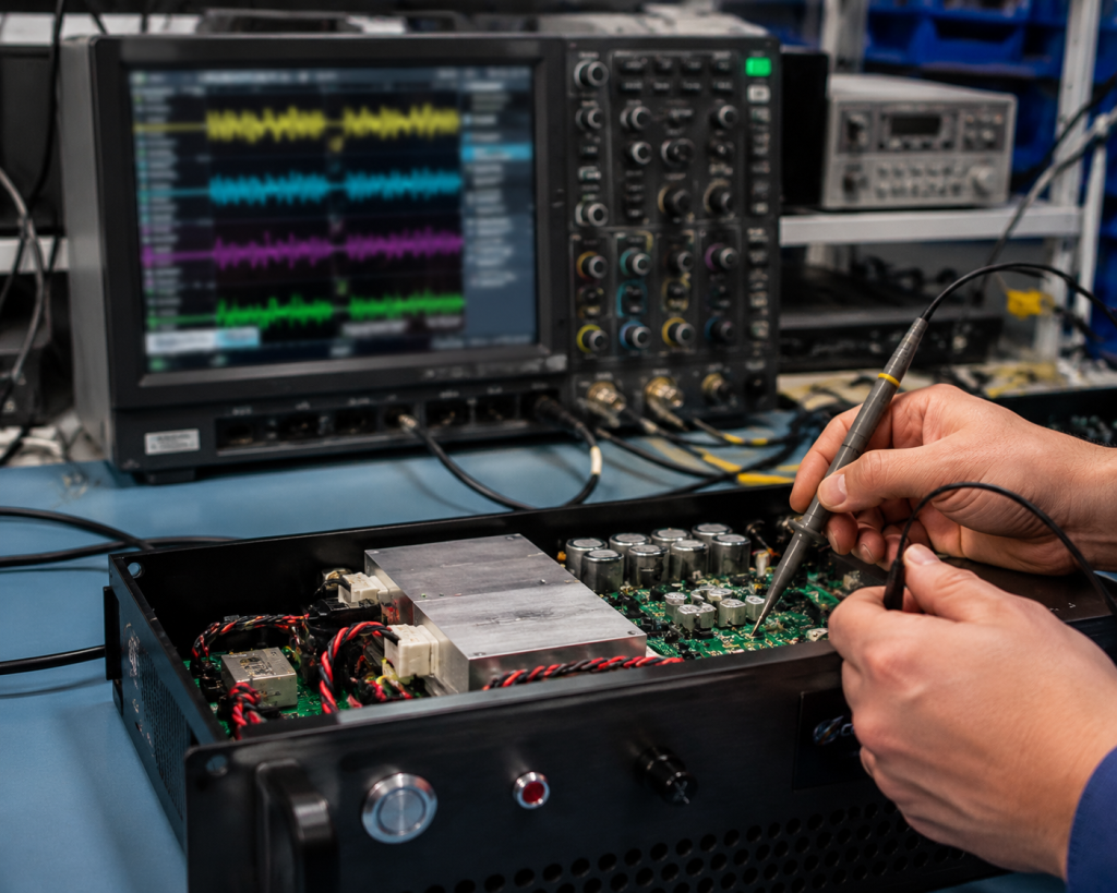
Probing power lines reveals hidden voltage fluctuations during system startup sequences. Technicians must connect probes directly across main supply input terminals. Monitoring supply rails identifies slow ramping issues causing sequence faults.
● Capturing Transient Spikes
Capturing transient spikes requires high-speed digital storage oscilloscopes. Slow meters completely miss microsecond voltage drops triggering component destruction. Triggering functions isolate exact moments when hardware failures begin.
● Analyzing Time Delays
Analyzing time delays between control signals prevents future hardware losses. Relays introduce unpredictable millisecond bouncing effects into active control lines. Solid-state logic circuits offer much tighter millisecond synchronization.
What exactly is the real story? We must capture exact microsecond timing events using high-speed digital storage oscilloscopes. Connect voltage probes directly across main supply terminals. Attach another probe near your signal generator trigger output port. Trigger your capture sequence based on primary main supply activation. Observe exactly when gate voltage stabilizes relative against incoming microwave pulses. A common mistake involves relying upon slow mechanical relay switching delays. You will often see excitation waves arriving while drain voltage remains zero. This specific mismatch confirms sequence-induced transistor destruction. Proper diagnostics isolate root causes rapidly. Imagine analyzing an active electronic warfare jammer pod failure. Connecting probes reveals main supply voltages ramping twenty milliseconds behind trigger commands. Review diagnostic logs from automated manufacturing test benches. Logs show signal generators firing test tones while amplifier bias planes remain grounded. Evaluate power transition states inside mobile command vehicles. Oscilloscopes display massive amperage spikes coinciding exactly with premature microwave pulse injections.
| Oscilloscope Channel | Monitored Point | Expected Timing | Fault Indicator |
| Channel 1 | Drain Voltage (VCC) | T=0 ms | High ripple |
| Channel 2 | Gate Bias (VGG) | T= -5 ms | Arrives late |
| Channel 3 | RF Excitation | T= +10 ms | Arrives early |
| Channel 4 | Current Draw | Steady rise | Massive instant spike |
3. Why Does GaN Technology Suffer From Improper Bias Sequencing?
● Depletion Mode Characteristics
Depletion mode characteristics dictate strict operational rules for modern power amplifiers. These semiconductors conduct maximum current continuously when gate voltage equals zero. Engineers must apply negative bias voltage before supplying main drain power.
● Pinch-Off Voltage Limits
Pinch-off voltage limits represent critical boundaries for safe transistor operation. Failing this precise sequence allows unlimited current flow through internal channels. Transistor junctions vaporize quickly under such extreme localized thermal stress.
● Junction Breakdown Mechanisms
Junction breakdown mechanisms involve rapid thermal runaway within microscopic semiconductor structures. Most commercial low-cost modules lack internal sequencing protection circuitry entirely. They depend entirely upon external controller accuracy for survival.
You might currently be wondering about this. Gallium nitride high electron mobility transistors operate primarily as depletion-mode devices. Our extensive field testing reveals consistent failures whenever system software glitches occur. You need hardware-level interlocks guarding these sensitive high-power microwave components. Protecting these expensive assets remains paramount for project success. A prominent defense contractor destroyed five prototype assemblies consecutively last month. They ignored GaN depletion characteristics while designing custom power distribution printed circuit boards. Telecom base station manufacturers learned this lesson through massive field recall campaigns. Missing negative voltage rails caused complete sector blackouts during routine maintenance cycles. Aerospace engineers testing satellite downlinks faced similar catastrophic semiconductor vaporization events recently. Software timing bugs enabled RF drivers before establishing safe transistor pinch-off voltages.
| GaN Device State | Gate Voltage | Drain Voltage | Channel Status |
| Standby | -5V DC | 0V | Pinched off (Safe) |
| Ready | -2.5V DC | 28V DC | Idle current flowing |
| Active | -2.5V DC | 28V DC | Amplifying signal |
| Failure Sequence | 0V | 28V DC | Massive short circuit |
4. How Does A VNA Trace Reveal Front-End Damage?
● High-Frequency Trace Collapse
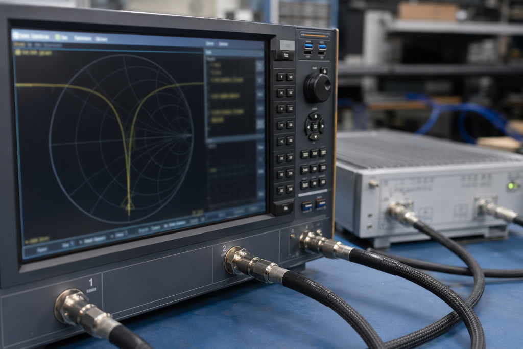
High-frequency trace collapse indicates severe physical damage inside input matching networks. Damaged front-end transistors cause total trace collapse specifically at higher frequency ranges. You will notice S11 approaching zero decibels near eighteen gigahertz marks.
● Return Loss Degradation
Return loss degradation provides early warning signs regarding component health. A healthy unit displays consistent return loss below negative fifteen decibels. Sweep frequencies across normal operating bands while monitoring S11 parameters.
● Identifying Matching Circuit Failures
Identifying matching circuit failures requires analyzing Smith chart impedance plots carefully. This flat-line response indicates melted input matching capacitors or wire bonds. Field technicians use this precise diagnostic method inside cramped radar vehicle bays.
This exact point is where things get interesting. A Vector Network Analyzer confirms hardware destruction without opening sealed enclosures. Connect your damaged module directly into VNA test ports carefully. Replacing cables wastes time when S-parameter measurements prove internal component death definitively. Accurate measurements prevent unnecessary repair delays permanently. One radar integrator noticed range degradation during live tracking exercises. VNA sweeps revealed totally flat S11 responses above fourteen gigahertz. This confirmed melted matching networks rather than simple antenna misalignment issues. An electronic countermeasure laboratory experienced mysterious output power drops. Connecting their damaged module into network analyzers exposed severe return loss degradation. The Smith chart displayed violent impedance swings near operating band edges. A university research team fried their primary testbed amplifier accidentally. Diagnostic sweeps showed normal low-frequency performance but complete signal reflection at higher bands. This frequency-selective failure proved internal transistor gate damage definitively.
| Frequency Band | Normal S11 (Return Loss) | Damaged S11 Trace | Diagnosis |
| 6,000 MHz | -18 dB | -10 dB | Partial degradation |
| 10,000 MHz | -20 dB | -5 dB | Severe mismatch |
| 14,000 MHz | -15 dB | -1 dB | Transistor gate short |
| 18,000 MHz | -16 dB | 0 dB | Complete catastrophic failure |
5. What Role Does DB9 Pin 3 Play In PTT Control?
● Push-To-Talk Logic
Push-To-Talk logic manages internal amplifier states through direct hardware control. Pin 3 handles Push-To-Talk functions requiring exactly 3.3 volts for activation. Keeping this pin at zero volts disables main amplifier stages safely.
● Voltage Thresholds
Voltage thresholds prevent accidental emissions during chaotic system startup phases. System integrators must wire their signal generator triggers directly through this specific connection. This physical interlock guarantees transistors remain inactive until RF drives stabilize completely.
● Preventing Unintended Transmissions
Preventing unintended transmissions protects downstream components from sudden power bursts. You cannot trust software timing loops running on loaded central processors alone. Hardware PTT lines react within nanoseconds during unpredictable system startup transient events. But wait, there is actually more. Proper hardware control logic saves systems from catastrophic sequencing errors easily. The CRF-PA-6000M18000M-100W utilizes an integrated DB9 interface for precise component management. This physical logic gate ensures absolute safety during power transitions. You save countless engineering hours by utilizing dedicated interlock pins. We helped an aviation control center redesign their entire transmitter rack. Routing master trigger pulses through DB9 interfaces eliminated all random startup failures. A commercial drone manufacturer struggled with payload burnouts during flight transitions. Utilizing hardware PTT lines synchronized power delivery perfectly despite software operating system lags. Military test ranges require absolute certainty regarding signal emission timing. Physical voltage thresholds provide foolproof protection against rogue processor execution threads.
6. Why Are Wideband Systems Particularly Vulnerable?
● Broad Frequency Parasitics
Broad frequency parasitics create unpredictable oscillations inside damaged matching networks. Managing a 6,000-18,000 MHz operating range requires complex internal matching networks. Wideband amplifiers present wildly different input impedances across their operational spectrum.
● Impedance Matching Complexities
Impedance matching complexities multiply across extreme multioctave operational bandwidths. Low-frequency signals might survive minor timing errors due to higher tolerance limits. However, eighteen gigahertz pulses interacting with unbiased transistors create destructive standing waves instantly.
● Power Saturation Variances
Power saturation variances cause massive thermal spikes when driven improperly. High-frequency energy reflects violently against mismatched internal boundaries during improper startups. These reflections compound existing thermal stress generated by incorrect DC power application.
Please consider this specific fact carefully. We see this specific phenomenon frequently during airborne drone payload testing procedures. Protecting wideband systems demands zero tolerance regarding strict operational timing delays. High standing wave ratios destroy internal transistors almost instantaneously. Strict adherence regarding activation delays prevents these costly accidents. Broadband jammers spanning multiple octaves require meticulous impedance control. Sending full power pulses across unmatched junctions creates massive localized heating. Satellite communication uplinks operating across wide Ku-bands face similar vulnerabilities. Reflected power from improper startup sequences destroys output combining networks rapidly. Spectrum monitoring stations utilizing ultra-wideband antennas demand robust front-end receivers. Transient standing waves during power cycles degrade low-noise amplifier noise figures permanently.
| Operating Band | Impedance Variation | Reflection Risk | Consequence |
| Low Band | Minor swings | Low | Recoverable heat |
| Mid Band | Moderate swings | Medium | Degraded lifespan |
| High Band | Severe swings | Extreme | Instant module death |
| Out of Band | Unpredictable | Critical | Cascading rack failure |
7. How Can Hardware Interlocks Prevent Sequence Mishaps?
● Internal Bias Sequencing
Internal bias sequencing removes reliance upon external operator timing accuracy completely. High-end units incorporate dedicated microcontrollers managing all internal power distribution silently. You supply twenty-eight volts while internal circuits generate necessary negative gate biases automatically.
● Over-Voltage Protection
Over-voltage protection circuits clamp deadly transient spikes before reaching sensitive components. The amplifier refuses main drain power until appropriate gate conditions exist fully. CorelixRF integrates complete over-voltage and VSWR protection directly into their circuit boards.
● VSWR Monitoring Circuits
VSWR monitoring circuits detect severe antenna mismatch conditions rapidly. These dedicated systems shut down operations upon detecting abnormal reflected power levels. Relying on integrated protection drastically reduces failure rates during complex multi-rack test array deployments. Are you ready for the good part? Advanced manufacturing prevents user error through smart internal hardware logic integration. These internal fail-safes provide immense value during frantic field operations. Engineers sleep better knowing hardware protects itself automatically. CorelixRF modules survived severe power grid fluctuations during remote desert testing. Internal voltage regulators maintained perfect gate bias while external supplies spiked unpredictably. An automated test facility shorted their main antenna feed accidentally. Built-in VSWR monitors deactivated amplifier stages instantly preventing any hardware damage. Shipborne radar systems face constant power quality issues at sea. Integrated protection logic guarantees safe operation despite terrible marine generator power characteristics.
8. What Are Key Specifications Of CRF-PA-6000M18000M-100W?
● 100W Output Power
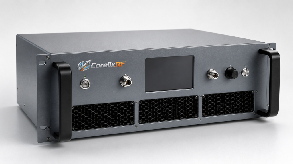
One hundred watts output power provides massive capabilities for long-range testing. The CRF-PA-6000M18000M-100W delivers one hundred watts across continuous wideband frequencies reliably. It utilizes a ruggedized SMA-Female input paired with an N-Female output connector.
● RS485 Communication Protocol
RS485 communication protocols enable robust telemetry inside noisy industrial environments. The integrated RS485 control interface allows precise remote monitoring via DB9 pinouts. Technicians track forward power, reverse power, and internal temperatures instantaneously.
● Aviation Cooling Design
Aviation cooling designs ensure stable thermal profiles during continuous wave operation. Built-in air cooling mechanisms maintain safe operating margins even under continuous wave test conditions. This unit targets demanding applications like electronic interference testing and aviation control networks. The honest truth must be told. Solving field failures requires selecting robust hardware designed for harsh realities. The integrated control mechanisms simplify complex field array deployments drastically. Data provided confirms operating parameters remain within safe engineering limits. Electronic warfare integrators deploy these units for continuous drone suppression operations. One hundred watts provides sufficient range for localized perimeter defense applications. Automotive testing laboratories utilize this specific model for radiated immunity validation. The wide frequency range covers numerous international compliance testing standards seamlessly. Research institutes driving specialized particle accelerators depend upon steady amplification. The RS485 interface allows seamless integration inside modern automated laboratory environments.
| Specification | Value | Unit / Protocol |
| Frequency Range | 6,000-18,000 | MHz |
| Rated Output Power | 100 | W |
| Gain | 50 | dB |
| Power Supply | DC 28V | Volts |
9. How To Validate System Stability After Component Replacement?
● Dummy Load Testing
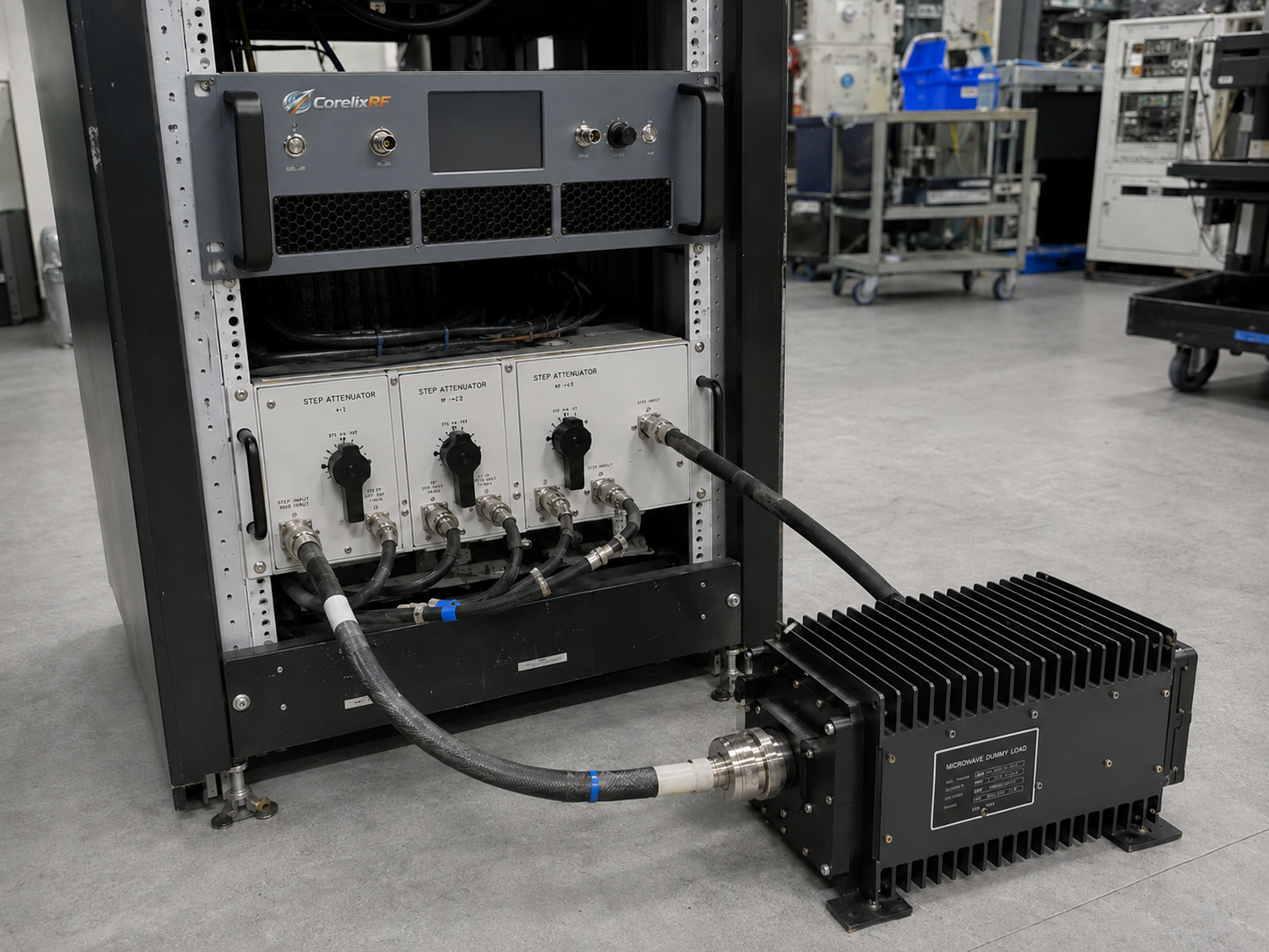
Dummy load testing absorbs massive energy safely during initial verification stages. Never connect a newly replaced amplifier directly into an untested antenna array. Always terminate your high-power output using an appropriately rated dummy load first.
● Step-Attenuator Calibration
Step-attenuator calibration manages drive levels preventing sudden over-saturation events. Utilize step-attenuators on your input feed increasing driving power gradually. Monitor DB9 Pin 6 for forward voltage tracking against applied excitation levels.
● Thermal Soaking Procedures
Thermal soaking procedures identify weak solder joints before final deployment occurs. A steady linear rise confirms stable internal amplification without sudden parasitic oscillation. Run continuous thermal soaking tests inside environmental chambers whenever possible before deployment.
The situation actually gets much better. Verification prevents repeating expensive mistakes caused by lingering upstream signal generation faults. Patience during this validation phase prevents repeating previous catastrophic failures. Thorough testing guarantees long-term reliability across demanding operational environments. A major telecommunications provider mandates twenty-four hour thermal soaking before field deployment. This practice identifies marginal components before they cause regional network outages. Defense contractors run full power continuous wave tests into high-power loads. Forward voltage tracking ensures output stability across all specified operating temperatures. Aviation engineers verify harmonic performance utilizing spectrum analyzers alongside step-attenuators. Gradual power application reveals subtle intermodulation distortion issues safely.
10. Why Should Integrators Mandate Strict Power-Up Protocols?
● Standard Operating Procedures
Standard operating procedures eliminate costly human errors during complex rack startups. Technology cannot completely replace disciplined operational engineering protocols inside testing facilities. Managers must enforce written startup checklists for every complex microwave array rack.
● Cost of Downtime
Costly downtime penalties destroy project budgets when critical amplifiers fail unexpectedly. Activating master breakers without verifying individual component states risks millions in damages. Training personnel regarding basic solid-state physics reduces accidental equipment destruction massively.
● Operator Training Requirements
Operator training requirements build a foundation for long-term hardware preservation. Engineers who understand depletion-mode semiconductor vulnerabilities naturally respect required timing constraints better. Treat high-power microwave systems with appropriate caution during every single laboratory initialization sequence.
Here is the final kicker. Professional B2B integration demands rigorous adherence towards proven technical methodologies always. Properly trained technicians rarely commit these specific sequencing errors. Establishing robust laboratory rules protects valuable microwave assets permanently. One radar facility reduced hardware failure rates ninety percent after implementing checklists. Visual verification regarding power switch positions saved thousands across quarterly maintenance budgets. A commercial testing lab fired technicians who bypassed mandatory safety protocols. Ignorance regarding high-power microwave physics costs companies massive financial penalties. Leading system integrators conduct mandatory semiconductor physics training classes annually. Educated operators treat expensive wideband amplifiers with appropriate professional respect.
Final Thoughts
Understanding strict RF drive and direct current sequencing prevents catastrophic field burnouts completely. Implementing hardware interlocks alongside robust component selection guarantees long-term operational stability. System integrators should adopt rigorous VNA verification procedures during troubleshooting phases. Master these engineering principles protecting your critical infrastructure permanently. Contact CorelixRF engineering teams today for detailed integration support regarding advanced GaN modules.
FAQ
Q1: What Causes Instant Burnout In Complex Integrated Systems?
Unsynchronized timing between direct current power supplies and microwave excitation signals destroys transistors.
Q2: How Do We Reconstruct Failure Scenes Using Oscilloscopes?
Engineers probe power lines alongside signal triggers capturing exact microsecond timing events accurately.
Q3: Why Does GaN Technology Suffer From Improper Bias Sequencing?
Gallium nitride transistors conduct maximum current continuously unless negative gate bias exists beforehand.
Q4: How Does A VNA Trace Reveal Front-End Damage?
Damaged units display total return loss trace collapses specifically near higher frequency limits.
Q5: What Role Does DB9 Pin 3 Play In PTT Control?
Pin 3 acts as physical hardware logic preventing transmission until correct voltage applies.