
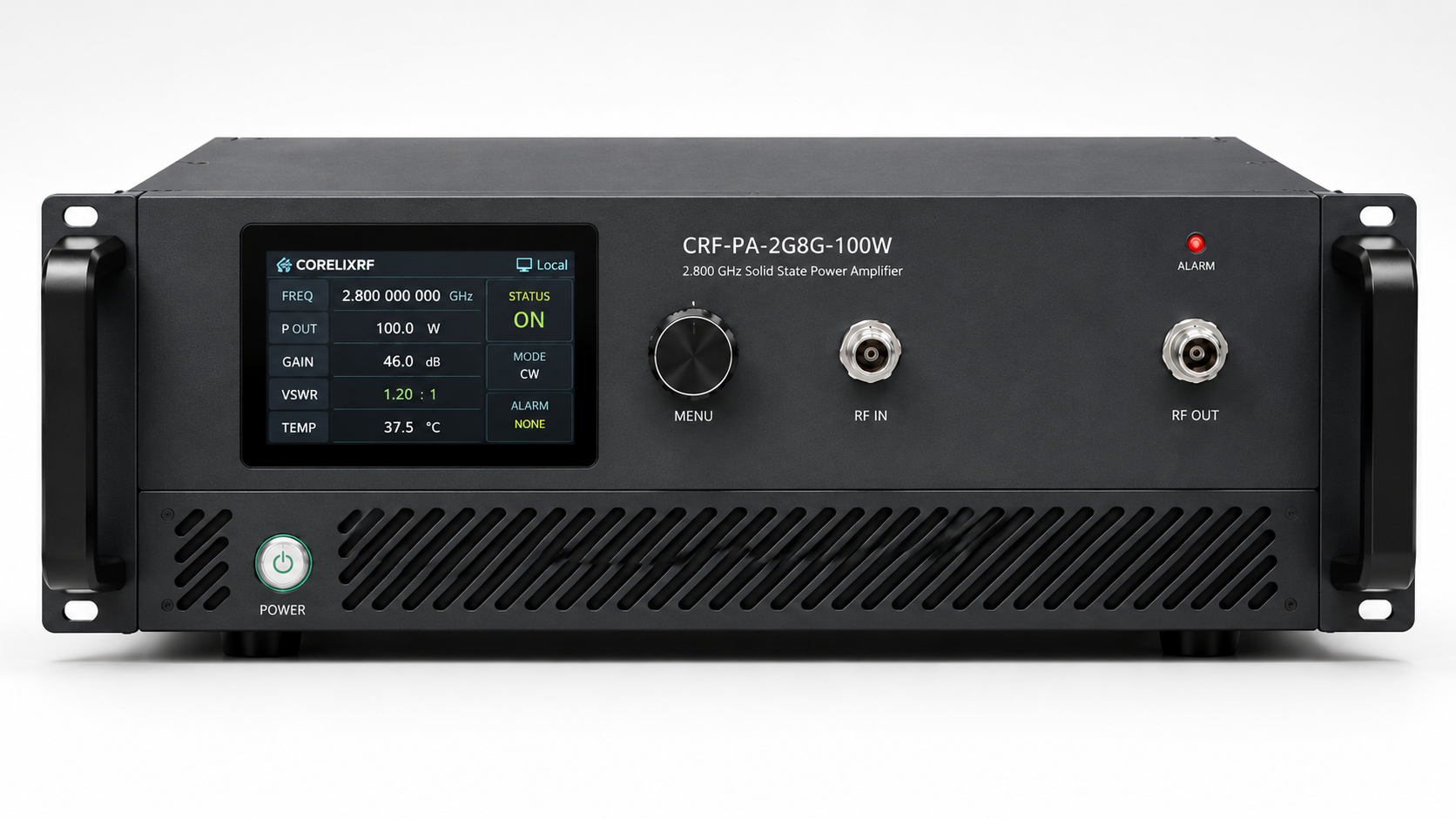
Architecture Analysis: Combating RF Amplifier Burnout From Power-On Sequencing in Complex Integrated Systems. System initialization failures destroy expensive communication arrays instantly. This article examines catastrophic hardware loss caused by incorrect power sequencing. We detail physical breakdown mechanisms and present robust integration methodologies protecting high-power amplifier modules during active deployment. Solving these complex issues requires absolute engineering truth.
1. What Causes Instant RF Amplifier Burnout During System Initialization?
Initialization Dynamics
System initialization failures cause catastrophic hardware loss inside complex radar arrays. Engineers watch oscilloscope screens flash red with over-current warnings. Transistors melt instantly when operators ignore strict power-up sequences. RF amplifiers demand precise gate bias timing before applying drain voltage. Applying a driving signal prematurely forces GaN devices into thermal runaway. Hardware destruction happens within microseconds during mismatched power state shifts. Here is the real deal. Real-world electronic warfare setups face chaotic power grid fluctuations continuously. Generators spooling up introduce massive voltage ripples across DC supply lines. Upstream processors boot faster than high-power amplification stages stabilize. This timing delta pushes unprepared circuits beyond maximum current ratings abruptly. Field technicians pulling charred 19-inch rack modules know this painful reality. We engineer systems with zero margin for lazy sequencing protocols.
Modern radar architecture relies upon distributed power grids spanning multiple vehicle bays. These long DC cable runs act like massive inductors resisting rapid current changes. When contactors slam shut transferring raw grid power into system racks chaos ensues. Huge inrush currents saturate line filters dropping nominal voltages across entire backplanes. Any sensitive RF module attempting a boot sequence during this voltage sag risks failure. Here is another factor entirely. Oscillators locked onto unstable reference rails output wildly varying frequencies during startup. Supplying these erratic tones into an unbiased amplification stage creates severe mixing products. These spurious emissions reflect backwards off unpowered output filters heavily. We mandate isolating high-power units behind dedicated power conditioning circuits strictly. A reliable RF signal chain demands rock-solid fundamental electrical foundations initially.
2. How Does DC Power Sequencing Impact High-Power RF Modules?
Component Level Stress
Radar base stations experience severe timing desynchronization between digital controllers and RF frontends. Command modules send excitation pulses before analog power rails reach nominal voltage. Solid-state amplifiers operate in depletion mode requiring negative gate pinch-off initially. Pumping microwave energy into an unbiased transistor gate ruptures internal junctions. Reflected energy compounds this failure by generating standing waves rapidly. What is the real story? Poor system architecture ignores transient responses during cold starts entirely. Designers specify cheap commercial power supplies lacking programmable delay circuits. These inadequate supplies overshoot voltage targets while charging massive decoupling capacitors. Component degradation accelerates exponentially under repeated improper power cycling events. Our engineering troubleshooting reveals identical failure modes repeatedly across degraded chassis. True engineering requires deterministic control over every millisecond during boot sequences.
Evaluating transistor datasheets reveals strict absolute maximum ratings regarding gate-to-source voltages. Operating outside these narrow margins punches microscopic holes through delicate oxide layers. These localized failures create resistive shorts bleeding precious bias currents toward ground. Over time a perfectly functional amplifier begins running hotter while delivering less power. Technicians misdiagnose these slow degradation faults blaming antenna mismatches incorrectly. Think about this serious problem. A single millisecond of improper sequencing shaves months off device lifespans. We measure these microscopic degradation signatures using advanced vector network analyzers constantly. Phase noise performance degrades measurably long before catastrophic thermal events occur. True factory-level manufacturing demands tracking every module through hundreds of power cycles rigorously. Only statistically sound power sequencing protocols guarantee long-term operational survivability.
System Diagnostics
| Sequence Error | Component Impact | System Level Symptom |
| RF Before DC | Gate Junction Rupture | Total Signal Loss |
| Drain Before Gate | Massive Current Draw | Blown Supply Fuses |
| Voltage Overshoot | Dielectric Breakdown | Magic Smoke Release |
3. Why Do Standard Power Supplies Fail in Radar and Electronic Warfare Architectures?
Power Supply Architecture
Commercial off-the-shelf power converters rarely survive inside active electronic warfare environments. These units feature sluggish transient recovery times under heavy dynamic loading. Radar pulse trains demand instant current delivery without voltage droop penalties. Standard switching supplies introduce excessive high-frequency noise into sensitive bias lines. You might be wondering now. Why do cheap converters destroy expensive RF payloads? The answer involves uncontrolled output ramping during initial AC grid connection. Cheap regulators lack hardware interlocks linking gate bias availability with drain power. A missing negative voltage rail leaves active devices fully conducting. Hundreds of amperes flow instantly through fragile semiconductor channels without restriction. Engineering truth dictates building dedicated sequencer boards featuring hardwired logic gates. Software delays cannot protect hardware against unexpected operating system crashes. Real systems demand physical interlocks preventing catastrophic current surges absolutely.
Switching power supplies utilize pulse width modulation techniques driving massive inductive loads. Poorly designed feedback loops oscillate wildly when suddenly connected against large capacitive loads. This oscillation manifests as severe voltage ringing riding atop DC supply rails. High-power amplification modules present highly dynamic impedance profiles during boot operations. A commercial supply sees this shifting load and reacts erratically. Consider the evidence presented here. We captured 50V rails spiking beyond 80V during uncontrolled initialization sequences. These massive over-voltage transients exceed absolute maximum drain ratings instantly. Capacitors explode while semiconductor junctions fuse into solid metallic blocks. Designing complex integrated systems requires custom linear power architectures featuring slow soft-start capabilities. Hardwired current limiting prevents any singular module from pulling down entire backplanes.
4. How Does Premature RF Excitation Destroy Gallium Nitride Transistors?
Solid State Physics
Gallium Nitride devices offer massive power density across wide frequency bands. This physical advantage becomes a severe liability during incorrect boot procedures. Pumping a +10 dBm microwave signal into an unpowered GaN stage causes havoc. The RF energy rectifies across unbiased junctions generating internal DC voltages wildly. Unintended channel conduction begins while external power rails remain completely off. This is where things get interesting. When main DC power finally arrives the transistor enters an undefined operating state. Massive thermal hotspots form instantaneously across localized semiconductor fingers. Heat cannot propagate into metallic baseplates quickly enough preventing crystalline structure vaporization. Destructive physical breakdown occurs faster than standard fast-blow fuses react. We mandate strict logic controllers enforcing an ironclad operational order always. Bias arrives first followed by drain voltage and finally excitation signals.
Gallium Nitride high electron mobility transistors trap charge carriers differently than legacy silicon. These deep-level traps require specific initialization routines preventing current collapse phenomena. Hitting a cold device with maximum microwave drive forces charges into structural defects. These trapped electrons alter internal electric fields pinching off conductive channels permanently. Output power drops massively even after normal DC conditions eventually arrive. Here is the ultimate kicker. Recovering from charge trapping requires complete power down and thermal equalization cycles. Electronic warfare scenarios cannot wait several minutes while arrays reset themselves. We combat these physics-level problems by strictly controlling energy application rates. Soft-starting RF drives prevents violent electron injection into semiconductor trap states. Our engineering methodologies respect solid-state physics rather than fighting physical limits.
Component Architectures
| Parameter | Commercial Supply | Engineering Grade Supply |
| Ramp Control | Unpredictable | Deterministic |
| Transient Noise | 150 mV p-p | < 10 mV p-p |
| Hardware Interlock | None | Dual Logic Gates |
5. What Are Hidden BOM Traps in Upstream Frontend Matching Networks?
Network Impedance Dynamics
System integrators often select frontend components based strictly on static S-parameters. They ignore dynamic impedance shifts occurring during amplifier power state shifts. An unpowered high-power module presents a massive impedance mismatch toward driver stages. Upstream oscillators face severe reflections bouncing back along transmission lines violently. These standing waves disrupt phase-locked loops causing massive frequency unlocking events. Let me explain this phenomenon. Drivers pushing energy into mismatched loads experience severe voltage standing wave ratios. Cheap isolators placed between stages saturate under continuous reflected energy loads. Magnetic ferrite materials heat up rapidly losing their directional isolation properties entirely. Component degradation spreads upstream destroying delicate digital-to-analog converters systematically. Rigorous bill of materials selection requires evaluating parts under full reflection conditions. Only robust circulators possessing adequate thermal mass survive these harsh realities.
Transmission lines connecting multiple system blocks possess specific characteristic impedances. Unpowered amplifiers behave like massive reflective walls bouncing energy back toward sources. Driver modules lack sufficient reverse isolation handling these massive returning power waves. Heat builds up rapidly inside driver final stages causing cascading chain failures. An entire rack goes dark simply because one downstream module booted slowly. Keep this specific fact in mind. We implement robust absorptive filtering mitigating these dangerous reflection coefficients actively. Utilizing high-power attenuator pads provides broadband matching regardless of active device states. These passive safety measures burn slightly more power while guaranteeing absolute system stability. Professional hardware design anticipates asynchronous boot conditions across distributed array architectures. Building resilient communication networks requires expecting individual block failures continuously.
6. How Do Engineers Diagnose Sequencing Failures Using Oscilloscopes and VSWR Meters?
Diagnostic Methodologies
Field technicians diagnosing burnt modules require specialized instrumentation tracing fast transient events. A standard digital multimeter updates too slowly capturing microsecond sequencing glitches. We deploy high-bandwidth oscilloscopes triggering on logic level power rail transitions. Current probes monitor absolute draw during the exact moment excitation begins. Here is a proven fact. Capturing a power-on anomaly requires setting precise trigger thresholds carefully. VNA traces show high-frequency roll-off characteristics collapsing after just one bad boot. Reflected power measurements spike violently when bias timings drift by milliseconds. Identifying root causes means charting every single voltage rail synchronously. Our engineers reject assumptions favoring hard empirical data gathered from ruined chassis. Hardware never lies about electrical abuse inflicted by poorly coded boot scripts.
Isolating intermittent power-up failures requires methodical data logging across multiple environmental conditions. Cold ambient temperatures change capacitor equivalent series resistance affecting voltage ramp times drastically. System integrators deploying hardware into freezing conditions experience completely different boot behaviors. We place test units inside environmental chambers running automated power cycling scripts continuously. Telemetry systems log every single current spike revealing marginal timing margins clearly. What happens next is shocking. Engineers overlay thermal maps against current logs identifying transient hot spots accurately. This granular data allows precision tuning of our internal sequencer delay times. We adjust gate bias application curves matching specific transistor lot characteristics perfectly. Guesswork has zero place inside high-reliability radio frequency hardware development labs. Empirical measurements drive every single design iteration from prototype toward final production.
Sequencer Timings
| Step | Action | Required Delay |
| 1 | Apply Gate Bias (-V) | > 10 ms |
| 2 | Apply Drain Voltage (+V) | > 50 ms |
| 3 | Enable RF Input | > 100 ms |
7. Why Does CRF-PA-2000M8000M-100W Solve Power-On Sequencing Problems?
Autonomous Controller Design
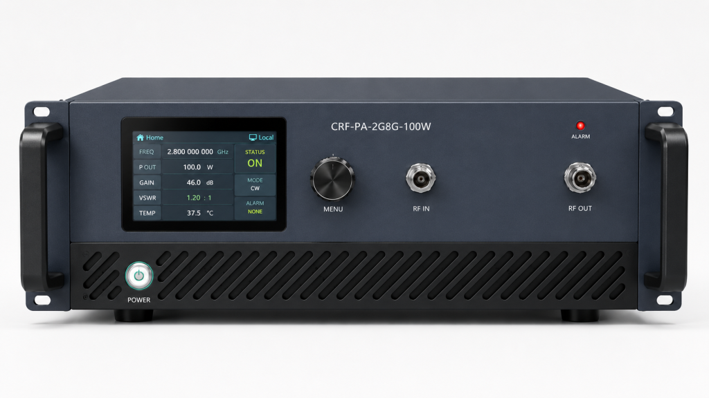
The CRF-PA-2000M8000M-100W specifically targets these exact system integration nightmare scenarios directly. Operating from 2000 MHz up through 8000 MHz this unit delivers stable output. Providing 100W of rated power demands rigorous internal power management architectures. We designed an internal logic controller handling all sequencing autonomously. Users simply apply main AC 220V power and let internal systems work. What does this mean for you? External command modules can send erratic signals without destroying internal GaN blocks. Our integrated sequencer establishes negative gate pinch-off before engaging massive drain supplies. An internal switch blocks external microwave energy until DC rails stabilize completely. This architecture physically prevents excitation from reaching active components prematurely. Moving control logic internally eliminates software-induced hardware failures entirely.
Our proprietary internal sequencer utilizes highly reliable microcontroller architectures running deterministic firmware. Watchdog timers monitor code execution preventing any software hang from freezing safety relays. Upon detecting grid power the controller activates negative voltage generators instantly. A dedicated analog comparator verifies gate bias reaches nominal levels before proceeding. Only after verifying pinch-off does the system energize massive drain supply contactors. Pay close attention to this. This sequential verification completely removes blind timing assumptions from system initializations. The unit communicates readiness statuses across RS485 interfaces updating external command computers. External systems must wait for this green light before transmitting drive signals. This handshake protocol eliminates chaotic asynchronous power application across complex arrays. We deliver plug-and-play reliability solving upstream architectural errors through localized smart hardware.
8. How Do Built-In Protection Circuits Mitigate Over-Drive and VSWR Faults?
Fault Tolerance Engineering
Beyond timing controls we implemented robust hardware protection guarding against external faults. A severed antenna cable creates infinite voltage standing wave ratios instantly. Conventional amplifiers reflect that 100W energy backwards vaporizing internal matching networks rapidly. The CRF-PA-2000M8000M-100W features high-speed directional couplers sensing reflected power continuously. Are you ready for the good part? Analog comparator circuits trigger shutdown routines within microseconds upon detecting anomalies. This hardwired protection overrides user commands preventing sustained damage from load mismatches. Over-drive scenarios trigger similar attenuation networks keeping active devices within safe operating areas. Input signals exceeding 0 dBm will not cause internal stage saturation. We prioritize equipment survival over maintaining transmission during catastrophic external network failures. Replacing a damaged antenna costs less than replacing an entire rack module.
Real electronic warfare deployments face continuous threats from hostile jamming and physical damage. Shrapnel severing a transmission line creates sudden open circuits during maximum power transmission. Our internal directional couplers detect this total reflection within nanoseconds reliably. High-speed PIN diode attenuators engage instantly dropping input drives below destructive thresholds. This reaction time beats any software-based polling loop running on external controllers. Why does this matter today? Surviving a direct antenna strike keeps allied communication networks online partially. Once technicians repair severed cables the amplifier resets automatically resuming normal operations. We include robust over-voltage clamping circuits absorbing grid transients efficiently. Lightning strikes nearby induce massive energy spikes across long supply cables frequently. Our ruggedized input stages dissipate these lethal transients keeping active GaN dies safe.
Hardware Specifications
| Parameter | Specification | Unit |
| Frequency Range | 2000 – 8000 | MHz |
| Rated Output Power | 100 | W |
| Gain | 50 | dB |
| Input VSWR | 2:1 | Ratio |
9. What Thermal Dissipation Strategies Protect 100W Amplifiers in 19-inch 3U Racks?
Thermodynamic Management
Packaging a 100W broadband amplifier inside a 19-inch 3U rack presents severe thermal challenges. Wasted energy transforms into heat needing immediate evacuation from sensitive semiconductor junctions. Stagnant air inside electronic warfare cabinets accelerates component degradation dramatically. We utilize precision-machined copper baseplates drawing heat away from GaN dies rapidly. Here is the bottom line. High-volume forced air cooling pushes massive CFM across custom extruded aluminum fins. Built-in over-temperature sensors monitor baseplate metrics triggering alarms before critical thresholds break. Thermal runaway cannot occur because hardware cuts drive signals upon detecting excess heat. Continuous wave operation across 2000 to 8000 MHz generates significant dissipation requirements. Our mechanical layout increases airflow while maintaining strict RS485 and LAN control isolation. Every chassis undergoes brutal burn-in cycles validating continuous operation under maximum thermal loads.
Operating continuously at 100 watts output power generates severe thermal loading dynamically. Gallium Nitride devices concentrate extreme heat across microscopic gate finger structures. Moving this concentrated thermal energy toward external heat sinks requires specialized metallurgical interfaces. We utilize highly conductive thermal compounds filling microscopic voids between packages and baseplates. This meticulous assembly process reduces thermal resistance drastically preventing localized die cracking. Here is the absolute truth. Fans alone cannot cool poorly mounted semiconductor devices adequately during summer deployments. Our 19-inch rack enclosure integrates precision-milled air channels guiding flow across critical zones. We monitor absolute baseplate temperatures cutting drive signals if cooling systems fail completely. Redundant thermal sensors eliminate single points of failure within our safety monitoring loops. True factory manufacturing guarantees consistent thermal performance across every delivered unit.
10. How Can System Integrators Verify Safe Initialization Sequences?
Integration Best Practices
System integrators must validate power sequencing before deploying active electronic warfare arrays. Connecting dummy loads instead of actual radiating antennas provides a safe testing baseline. Engineers monitor RS485 telemetry outputs verifying internal state machines operate correctly. A properly integrated system shows zero output spikes during cold start initializations. Truth be told right now. Skipping these validation steps leads directly toward expensive field failures eventually. We highly recommend utilizing directional couplers capturing transient RF energy during boots. Monitoring actual current draw verifies internal bias circuits function as engineered. Our factory testing utilizes identical verification matrices guaranteeing out-of-box reliability unconditionally. Professional manufacturing means delivering equipment capable of surviving hostile electrical environments flawlessly. We build RF hardware designed for reality instead of idealized laboratory conditions.
System architects must implement hardwired interlocks between RF signal generators and amplifier chassis. Software commands sent over local area networks introduce unpredictable latency during emergency shutdowns. A physical copper wire dropping logic levels acts faster than any digital packet. We provide dedicated interface pins allowing instant mute capabilities externally. Integrating these hardware mutes into global safety loops prevents cascading array failures. Make no mistake about this. Trusting complex software handling microsecond hardware timings guarantees eventual catastrophic destruction. We supply detailed mechanical drawings guaranteeing proper rack integration and airflow planning. Following our documented spacing guidelines prevents thermal choking inside dense equipment cabinets. CorelixRF delivers uncompromising engineering truth supporting your most critical mission requirements. Reach out for detailed system-level evaluation data regarding our high-power solutions.
Deployment Metrics
| Feature | Description | Reference |
| Package Size | 19-inch 3U | |
| Cooling Method | Air cooling | |
| Operating Temp | 0 – 50 °C | |
| Interfaces | RS485 / LAN |
Final Engineering Assessment
System integrators must respect solid-state physics when designing complex radar backplanes. Proper gate bias timing prevents catastrophic hardware destruction unconditionally. Our CRF-PA-2000M8000M-100W model delivers autonomous sequencing protecting your mission-critical payloads effectively. Contact CorelixRF engineering teams today for advanced integration support and detailed technical specifications regarding our high-power amplification solutions.
FAQ
Q1: What causes instant RF amplifier burnout during system initialization?
Applying microwave drive signals before establishing proper negative gate bias causes massive unregulated current flow through GaN transistors.
Q2: How does DC power sequencing impact high-power RF modules?
Improper DC sequencing creates thermal runaway conditions because unbiased semiconductor junctions cannot block massive inrush currents from main supplies.
Q3: Why do standard power supplies fail in radar and electronic warfare architectures?
Commercial supplies lack deterministic hardware interlocks and suffer from severe voltage ringing when charging massive capacitive loads during boots.
Q4: How do built-in protection circuits mitigate over-drive and VSWR faults?
Internal directional couplers detect reflected energy instantly triggering high-speed analog comparators that cut drive signals before thermal destruction occurs.
Q5: How can system integrators verify safe initialization sequences?
Engineers must utilize high-bandwidth oscilloscopes measuring actual current draw transients alongside directional couplers monitoring RF reflections during cold starts.