
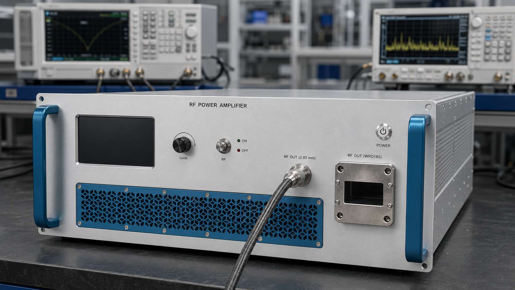
Complex integrated platforms frequently suffer from catastrophic component failures during startup procedures. Engineers face immense pressure when expensive field-replaceable units vaporize within milliseconds after flipping main breakers. Smoke pouring from a chassis indicates massive thermal runaway resulting from incorrect voltage application sequences across high-frequency transmit chains. Here’s the deal, operating advanced gallium nitride amplifiers demands absolute precision regarding when bias voltages reach specific semiconductor terminals. Applying radio frequency drive signals before establishing strong negative gate pinches forces unmitigated drain currents through fragile transistor junctions. Those currents generate localized hotspots exceeding material breakdown thresholds almost instantly. Our manufacturing facility leverages thirty years of historical field data alongside four hundred dedicated engineering personnel addressing these exact physical breakdowns. We implement rigorous structural hardware solutions preventing sequencing catastrophes within demanding electronic warfare environments. System integrators require absolute reliability replacing vulnerable discrete components with protected assemblies.
1. What causes complex integrated systems to experience catastrophic front-end failures?
The hook and field restoration
System startup phases present extreme vulnerability windows for high-power microwave assemblies operating across 18,000 through 40,000 MHz bands. Radar technicians staring at spectrum analyzers often witness devastating intermodulation spikes followed immediately by complete noise floor collapse. That specific trace collapse signifies total device destruction inside your primary transmit block. You might be wondering, why do standard laboratory power supplies fail at protecting field-deployed hardware? Laboratory environments utilize gentle ramp rates alongside controlled single-channel activations. Field deployments force simultaneous main bus engagements across multiple interacting subsystems simultaneously. High-frequency vibration profiles combined with salt fog intrusion create unpredictable impedance shifts at antenna ports. These environmental factors reflect massive standing waves back into unprotected output stages during sensitive transient states. Mismatched excitation timing compounded by antenna mismatch practically guarantees solid-state device vaporization.
DC power supply sequencing errors
Improper direct current application logic remains a primary killer of advanced broadband amplification modules. Gallium nitride technology requires negative gate voltages applied prior applying high positive drain potentials. When integrators link main distribution buses directly across amplifier terminals without intelligent delays, massive current spikes occur. What’s the real story? Cheap commercial sequencers experience millisecond-level jitter during cold starts or extreme thermal fluctuations. That tiny jitter interval allows full drain voltage presence while gate terminals remain floating near zero volts. Depletion-mode devices naturally rest in an open-channel state allowing maximum electron flow. Millions of electrons flood across microscale gate channels generating temperatures exceeding 800 degrees Celsius instantly. Bond wires melt rapidly while semiconductor crystalline structures fracture permanently. Proper architecture demands dedicated hardware-level timing controls physically built inside enclosed amplifier modules.
RF excitation timing mismatches
Applying microwave drive signals prematurely creates another distinct failure mode inside complex arrays. Synthesizers powering up faster than downstream power blocks inject high-level signals into unpinned transistor junctions. Forward-biased gate conditions draw excessive RF currents exceeding maximum safe operating area limits. Ready for the good part? True engineering practice dictates holding drive signals completely muted until all amplifier stages report stable quiescent current states. A common integration mistake involves routing master oscillators through passive splitters directly into active transmit chains. When that master oscillator initializes, RF energy propagates outward regardless of downstream amplifier readiness. Unbiased amplifiers present highly mismatched input impedances reflecting significant energy backwards. This creates severe standing wave ratios disrupting entire system phase coherency. Hardware selection must prioritize modules featuring integrated RF input threshold limiting alongside active overdrive protection circuits.
System Failure Modes | Manifestation | Root Cause
Catastrophic Burnout | Smoke / Odor | Drain voltage applied before gate pinch-off
Trace Collapse | Sudden gain drop on VNA | RF overdrive during DC sequencing
Thermal Runaway | Chassis overheating | Sustained high quiescent current from jitter
Phase Distortion | Irregular radar pulses | Unbiased amplifier reflecting master oscillator energy
2. Why do depletion-mode GaN transistors require strict power-on matching logic?
Gate pinch-off voltage dependencies
Wideband high-power applications rely heavily upon gallium nitride high electron mobility transistors for superior power density. These specialized transistors feature a naturally open conduction channel requiring active voltage control for current suppression. This is where it gets interesting, negative bias applied at gate terminals pinches off this conduction path effectively halting electron flow. Applying standard 28V or 50V drain potentials without that protective negative gate barrier results in unlimited current draw. The resulting instantaneous power dissipation far exceeds thermal transfer capabilities of typical copper-tungsten flange materials. Engineers designing electronic warfare suites must understand these fundamental physical limitations when specifying system-level block diagrams. Relying on software-defined timing loops introduces unacceptable latency risks during rapid field deployments. True reliability necessitates hardware-level gate-first logic permanently embedded within primary amplifier control boards.
Drain current thermal runaway mechanisms
Thermal dynamics within semiconductor junctions operate on microsecond timescales far faster than bulk chassis temperature changes. When gate sequencing fails, localized heating decreases electron mobility while simultaneously increasing leakage currents. This positive feedback loop accelerates rapidly until catastrophic junction failure occurs. Here’s the kicker, typical baseplate temperature sensors completely miss these microscopic thermal events. Thermistors mounted near amplifier housings react over seconds while transistors melt within milliseconds. System integrators frequently misdiagnose these failures blaming inadequate system cooling instead of addressing core timing flaws. Implementing robust hardware logic prevents these runaway scenarios regardless of ambient environmental conditions. A properly designed amplifier module internally monitors its own drain currents reacting autonomously. Shutting down internal bias networks before thermal limits are breached saves expensive hardware from inevitable destruction.
Analyzing system integration BOM blind spots
Procurement teams building bill of materials lists often overlook hidden integration costs associated with bare amplifier pallets. Purchasing discrete RF pallets forces system designers into building custom sequencer boards and protection networks. Those custom networks rarely undergo rigorous environmental stress testing compared against mature factory-integrated solutions. Truth be told, scattered component architectures increase overall system failure probabilities exponentially. Every additional connector, timing relay, and voltage regulator introduces another potential point of failure. Complex radar architectures demand consolidated modules containing fully verified internal logic handling all dangerous transient states. Our factory engineers evaluate hundreds of failed third-party integration attempts featuring overly complex discrete timing boards. Selecting fully enclosed subsystems eliminates these BOM blind spots entirely while drastically reducing system development timelines.
BOM Selection Comparison | Discrete Pallet | Integrated Module (CRF-PA)
Sequencing Logic | Customer developed | Factory embedded
Protection Speed | Milliseconds | Microseconds
Thermal Tracking | External sensors | Internal junction monitoring
Failure Probability | High | Extremely Low
3. How does improper hardware selection compromise radar and electronic warfare systems?
Link budget deterioration
Initial laboratory tests might show acceptable output power levels despite marginal sequencing logic implementation. Field conditions rapidly degrade these fragile setups causing severe link budget deterioration over time. Repeated minor timing violations cause slow degradation of transistor transconductance dropping overall module gain silently. Let’s look at the facts, operators notice decreased radar detection ranges without any active system fault alarms triggering. This silent degradation proves far more dangerous than immediate catastrophic failure during critical missions. Electronic warfare jammers losing 3dB of output power effectively halve their operational suppression radius. System integrators must prioritize hardware featuring verified long-term stability against transient stress events. Factory-calibrated modules maintain strict gain flatness across entire 18,000 through 40,000 MHz bands despite thousands of power cycles. Proper component selection guarantees consistent microwave link budgets matching initial system design parameters precisely.
High-frequency vibration and salt fog impacts
Naval and airborne platforms subject electronic components toward extreme physical punishment continuously. High-frequency vibrations loosen poorly secured discrete timing boards causing intermittent sequencing faults during active flight. Salt fog penetrates standard enclosures altering impedance characteristics across exposed microstrip transmission lines. You might be wondering, how do these physical stressors interact with startup sequencing vulnerabilities? Intermittent connections cause rapid, uncontrolled power cycling which standard commercial sequencers cannot handle. Those rapid cycles trigger false RF drives while gate voltages lag behind due to added capacitance from moisture. Hermetically sealed RF front-ends featuring integrated protection logic remain completely immune against these external environmental factors. Shielding sensitive timing circuits inside massive aluminum housings guarantees reliable performance during violent mechanical shocks.
VNA and spectrum analyzer diagnostic signatures
Troubleshooting compromised systems requires specific knowledge regarding failure signatures displayed across standard RF instrumentation. Vector network analyzers connecting toward damaged amplifier inputs typically show massive return loss degradation across specific frequency bins. This indicates physically melted input matching networks caused by severe RF overdrive events. What’s the real story? Spectrum analyzers monitoring output ports often display elevated broadband noise floors even when input signals remain absent. That specific noise floor elevation points directly toward compromised gate structures leaking excessive quiescent currents. Identifying these precise signatures allows field engineers pinpointing timing logic failures instead of blaming external system variables. Replacing damaged components requires selecting upgraded hardware featuring built-in VSWR protection alongside strict input limiting. Modules displaying flat S21 curves post-stress testing validate superior internal engineering practices.
Diagnostic Signature | Instrument | Physical Meaning
High S11 Return Loss | Vector Network Analyzer | Damaged input matching / RF overdrive
Elevated Noise Floor | Spectrum Analyzer | Compromised gate structure / leakage
Gain Compression | Power Meter | Degraded transconductance from thermal stress
Phase Noise Increase | Signal Analyzer | Unstable internal bias regulation
4. What physical mechanisms define CRF-PA-18000M40000M-70W solutions for power sequencing?
Introducing CRF-PA-18000M40000M-70W parameters
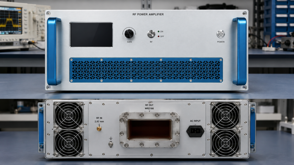
The CRF-PA-18000M40000M-70W wideband RF power amplifier delivers 70 watts rated output power across an 18,000 through 40,000 MHz spectrum. It features an impressive 49 decibel gain figure requiring merely 3 dBm input drive for full saturation. This is where it gets interesting, operating at these extreme millimeter-wave frequencies requires massive continuous power consumption reaching 1600 watts. Managing that incredible energy transfer demands an architecture built entirely around physical stability. Housed within a standard 19-inch 8U rackmount chassis weighing 40 kilograms, this unit commands physical presence. It utilizes a direct AC 220V power supply eliminating any need for vulnerable external DC sequencing logic. The input utilizes a precision 2.92mm female connector while output energy flows through robust WRD180 waveguide flanges.
Built-in protection architecture
CorelixRF engineering logic embeds strict protection mechanisms directly onto internal control motherboards. Whenever operators supply AC main power, an internal microcontroller boots independently verifying all environmental sensor data. This controller initiates a strict hardware-locked sequence establishing negative gate potentials prior energizing massive high-current drain supplies. Ready for the good part? Continuous monitoring circuits track over-voltage, over-temperature, and over-current states simultaneously at microsecond polling rates. If system integrators accidentally route high-level RF signals early, optional over-drive protection clamps input power instantly. The module automatically triggers full internal shutdown protocols protecting sensitive internal GaN devices without relying upon external commands. This self-contained defensive architecture completely eliminates human error regarding power-on sequencing mistakes during stressful field operations.
Resolving high-frequency matching issues
Millimeter-wave frequencies present unique challenges regarding impedance matching across wide bandwidths. Any slight physical variance within microstrip traces causes massive reflection coefficients at 40,000 MHz. CorelixRF utilizes proprietary high-frequency PCB materials alongside precise automated bonding wire techniques maintaining a strict 2:1 input VSWR. Truth be told, achieving an 8 decibel gain flatness across this massive spectrum requires intense physical modeling. We avoid flamboyant marketing claims preferring rigorous engineering truth backed by solid S-parameter test files. Reflected energy from mismatched antennas encounters massive internal circulators routing dangerous standing waves toward dedicated dump loads. This physical architecture allows continuous operation even when upstream system integrators deploy sub-optimal transmission lines. Our 400-person factory staff verifies every single unit against demanding baseline specifications guaranteeing absolute reliability.
CRF-PA-18000M40000M-70W Specifications | Parameter | Value
Frequency Range | Bandwidth | 18,000 – 40,000 MHz Rated Output Power | CW Power | 70 W Gain Characteristics | Small Signal | 49 dB (Max ±8 dB Flatness) Internal Protection | Embedded Logic | Over-voltage, Over-temp, Over-current
5. How do engineers integrate CRF-PA-18000M40000M-70W into existing frameworks?
Control interfaces and telemetry
Modern electronic warfare suites require deep telemetry integration allowing central computers full visibility into RF block statuses. The CRF-PA-18000M40000M-70W provides robust RS485 and LAN interfaces facilitating instant communication with master controllers. Engineers simply connect standard network cables mapping IP addresses for immediate digital access. Here’s the deal, reading real-time forward power, reverse power, and internal temperature states becomes a trivial software task. This digital transparency allows system integrators building complex phased arrays maintaining perfect synchronization across dozens of independent modules. Adjusting internal gain parameters up through 15 decibels happens digitally without requiring physical attenuator pads. Our protocol documentation provides clear hexadecimal commands eliminating ambiguous integration guesswork during critical project phases.
Thermal dissipation layout strategies
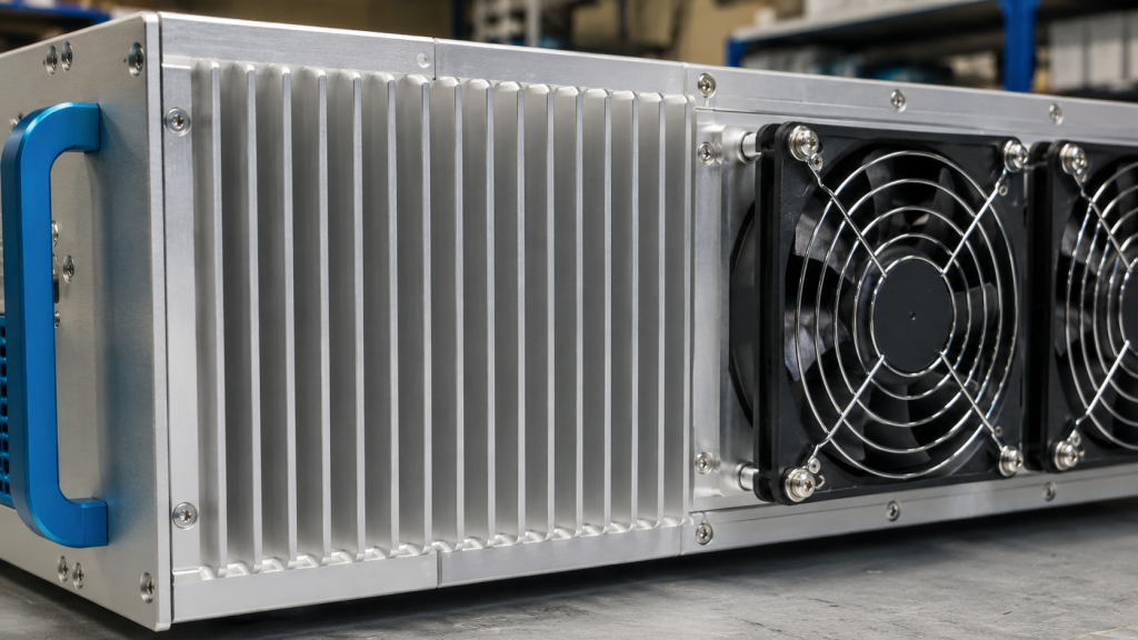
Dissipating 1600 watts of consumed electrical power requires massive forced air cooling methodologies. The 8U chassis design incorporates heavy-duty industrial fans driving enormous air volumes across deeply finned aluminum heat sinks. Rackmount installations must guarantee unrestricted airflow across front intakes and rear exhaust ports constantly. What’s the real story? Stacking multiple units closely together without adequate vertical spacing creates localized thermal vortexes trapping hot exhaust. System architects must calculate total HVAC cooling tonnage accurately when deploying several units inside mobile command shelters. Operating safely between zero and fifty degrees Celsius ambient temperatures depends entirely upon proper external airflow management. Our mechanical engineers provide detailed CAD models outlining optimal spacing requirements preventing thermal throttling during sustained high-power transmissions.
Validating performance metrics
Final system acceptance requires rigorous validation against published datasheet parameters using calibrated laboratory equipment. Connecting a directional coupler alongside high-power attenuators protects sensitive spectrum analyzers during full 70-watt output testing. Injecting a swept continuous wave signal verifies strict adherence towards specified -10 dBc harmonic levels. Let’s look at the facts, verifying spurious emissions below -60 dBc proves exceptional internal filtering architecture design. Engineers must utilize proper torque wrenches securing 2.92mm connectors preventing microscopic air gaps from destroying high-frequency performance. We supply detailed test data alongside specific pattern files aiding project review boards during critical buy-off stages. Relying on concrete empirical data builds absolute trust between our factory floor and frontline radar operators.
Integration Checklist | Action | Requirement
Airflow Management | Rack placement | Verify 8U clear intake/exhaust paths
Telemetry Connection | Interface wiring | Connect RS485 or LAN for remote monitoring
Output Termination | Load connection | Verify WRD180 waveguide flange torque
Performance Validation | Instrument test | Run swept CW verifying 70W at 40,000 MHz
Final Engineering Assessment
Eliminating catastrophic front-end burnout requires abandoning vulnerable discrete component integration strategies entirely. Designing complex integrated setups mandates selecting fully protected amplifier architectures featuring embedded power-on sequencing logic. We provide engineered solutions preventing thermal runaway alongside severe RF overdrive destruction during critical system deployments. Contact our technical team obtaining detailed documentation evaluating CRF-PA-18000M40000M-70W implementations for advanced microwave applications. Reviewing factory test patterns helps clarify complex integration uncertainties rapidly.
Q1: What is the main cause of amplifier burnout during system startup?
Applying drain voltage before establishing negative gate pinch-off forces massive unchecked current through GaN transistors, causing instantaneous thermal runaway.
Q2: How does the CRF-PA-18000M40000M-70W handle power sequencing?
It features internal microcontrollers that automatically establish gate bias before routing massive drain currents, eliminating reliance upon external sequencers.
Q3: What happens if high-level RF drives hit an unbiased amplifier?
Unbiased junctions present massive impedance mismatches reflecting energy backwards, creating severe VSWR conditions while destroying fragile semiconductor input structures.
Q4: Why are external thermistors insufficient for preventing thermal runaway?
External baseplate sensors react over several seconds, whereas microscopic semiconductor junction temperatures exceed material limits within tiny milliseconds during sequencing faults.
Q5: Can operators adjust gain remotely on the CRF-PA-18000M40000M-70W?
Yes, operators can digitally adjust internal gain up through 15 decibels utilizing standard RS485 or LAN telemetry interfaces.
Make the lab setup and report curves part of the RFQ
Test-bench issues become easier to resolve when the RFQ lists signal source, cable loss, load condition, calibration setup, power sequencing, gain flatness, spurious limits and report format.
Recommended next step: send the operating band, output power target, duty cycle, load condition, control interface, protection or thermal limits and required FAT documents. CorelixRF can review this How to Design RF Front-End Power Sequencing for Radar Systems? requirement against standard RF amplifier platforms, RF front-end options and controlled customization paths.