
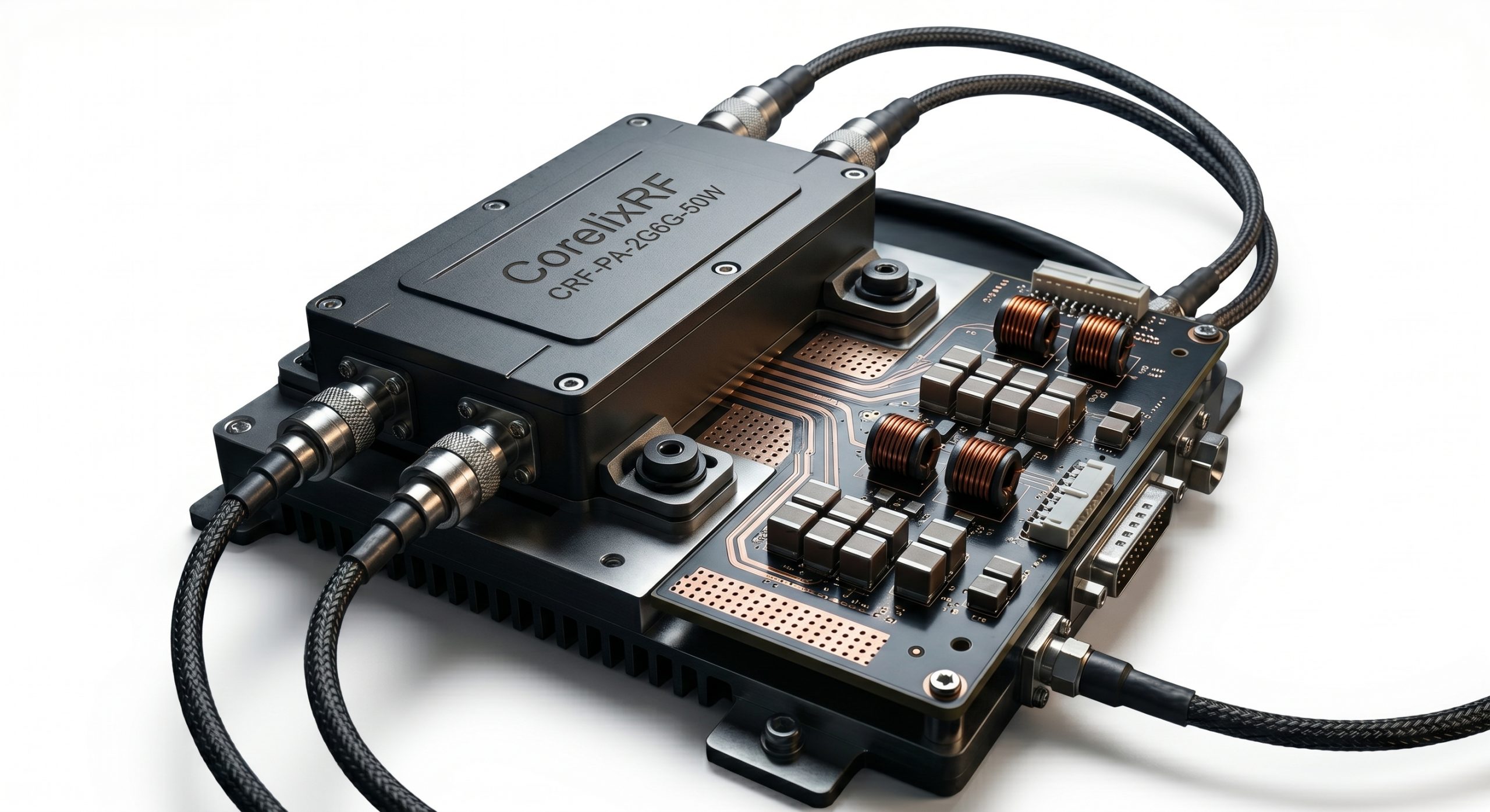
Operating within the demanding environment of modern aerospace systems exposes sensitive radio frequency hardware to hostile electrical conditions. The core engineering problem lies in the raw physical fact that raw electrical fluctuations act as a destructive modulation source when they reach active amplification devices. System integrators routinely battle severe voltage variations cascading across the power bus, directly interfering with the sensitive bias lines of high-frequency microwave modules. These unmitigated low-frequency alternating current components inject chaotic phase and amplitude variations directly into the communication signal path.
The mechanical and electrical consequences of ignoring this switching noise are catastrophic for airborne platforms. When this unconditioned power interacts with the high-gain stages of an amplifier, the resulting ordinary switching power supply ripple deteriorating RF EVM and spurious spectrum causes immediate communication link failures. Transistors are pushed violently out of their linear operating regions, resulting in the generation of massive intermodulation products that blind adjacent receivers. The resulting data packet loss completely paralyzes avionics data link operations, rendering targeting systems and secure telemetry channels effectively useless under dynamic flight loads.
To physically halt this electrical degradation, engineers must abandon commercial-grade workarounds and implement specialized hardware defense mechanisms. CorelixRF designs and manufactures heavily hardened microwave modules tailored for absolute survival in these exact harsh environments. By rigorously analyzing laboratory data and applying advanced physical materials, we enforce a pristine electrical baseline that guarantees flawless transmission. Our strict engineering approach neutralizes external power bus hostility, allowing systems to operate continuously without experiencing spectral breakdown.
Why Does Switching Ripple Degrade Avionics Data Link EVM?
Consider the physical reality The integration of modern avionics systems demands highly efficient power conversion, typically achieved through switching-mode power supplies operating at rapidly varying duty cycles. However, the operational switching frequencies of these power supplies generate massive low-frequency ripple currents that propagate directly into the system architecture. Implementing an Avionics Power Distribution Network (PDN): Power-side Termination Filtering Strategy to Ensure RF Spectrum Purity of 50W Broadband Amplifiers becomes a mandatory requirement rather than an optional design guideline. When ordinary switching power supply ripple interacts with the bias circuitry of a GaN transistor, the amplitude modulation and phase modulation effects actively deteriorate the radio frequency Error Vector Magnitude (EVM). This interaction forces the amplifier to operate outside its linear region, generating intermodulation distortion products that mask the actual digital modulation scheme used in the avionics data link. Engineers frequently observe a complete collapse of the constellation diagram during high-power burst transmissions, directly attributable to the unchecked voltage fluctuations reaching the drain terminal of the primary amplification stage, causing unrecoverable data link dropouts and violating strict military mission parameters.
How Does Low-Frequency Noise Translate to Spurious Emissions?
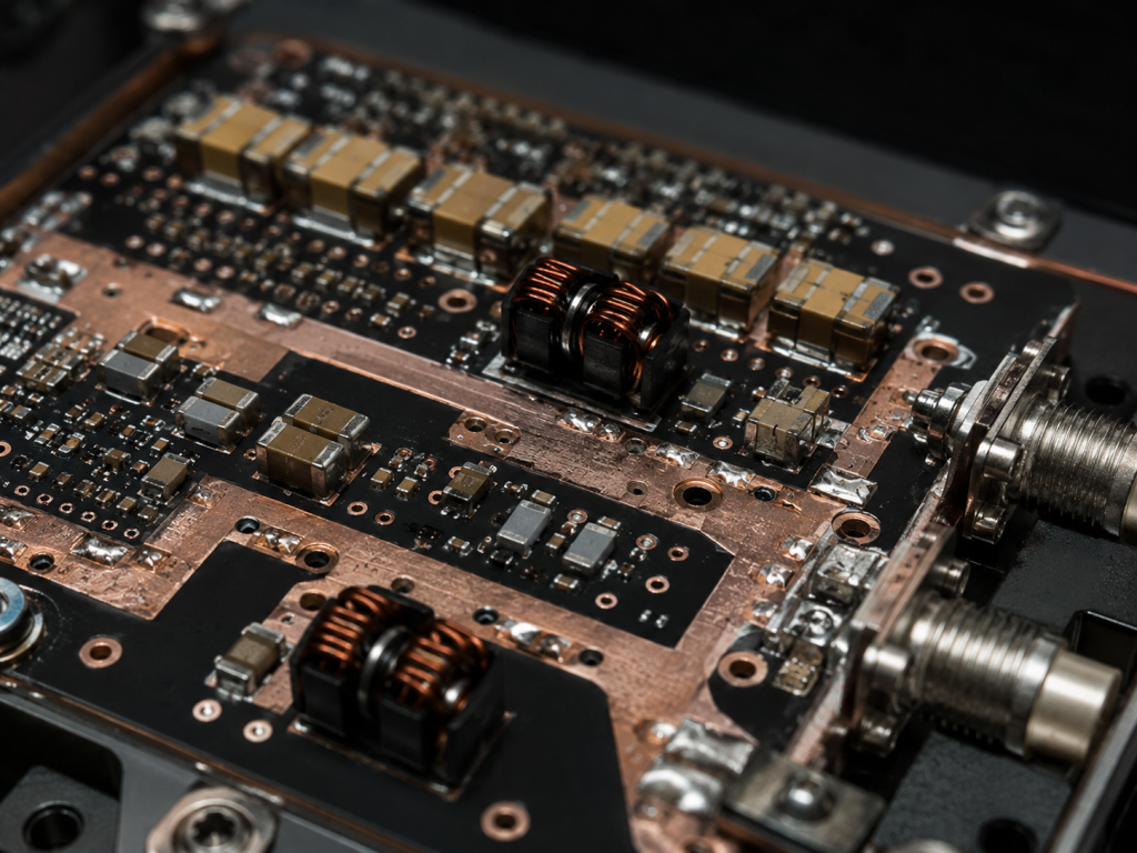
The fundamental physics dictate any nonlinear active device will mathematically mix incoming signal frequencies with bias line noise. When unmitigated power supply ripple reaches the RF amplification stages, the physical transistor acts as a high-power mixer. The baseband noise upconverts around the carrier frequency, manifesting as closely spaced spurious emissions that immediately violate stringent airborne communication regulatory standards. During our extensive laboratory stress testing on legacy amplifier architectures, introducing a mere 50mV peak-to-peak ripple on a 28V supply line generated spurious sidebands measuring -40dBc relative to the main carrier. These out-of-band emissions directly interfere with adjacent avionics receivers, causing massive packet loss and drastically reducing the effective range of the communication link. To strictly combat this phenomenon, precision filtering networks utilizing high-Q ceramic capacitors and custom-wound heavy-copper ferrite chokes must be deployed precisely at the module power entry point. This localized decoupling strategy successfully shorts the low-frequency noise components directly to the massive system ground plane before they can couple into the sensitive RF path, thereby maintaining a pristine spectral output even under highly aggressive dynamic loading conditions.
| Parameter | 20mV Ripple Impact | 50mV Ripple Impact | 100mV Ripple Impact |
| EVM Degradation | 1.2% | 3.5% | 8.9% (Link Failure) |
| Spurious Emissions | -55 dBc | -40 dBc | -25 dBc |
| Phase Noise Shift | < 1 dB | 3.5 dB | > 10 dB |
| Spectral Mask | Pass | Marginal | Fail |
What Is The Physical Impact Of Impedance Mismatch At The Power Terminal?
Let’s examine the raw data impedance mismatches at the high-current power supply terminal create catastrophic reflection coefficients that destabilize the entire amplification module assembly. In broadband applications spanning the 2GHz to 6GHz spectrum, the instantaneous current draw fluctuates wildly depending on the input signal modulation envelope. If the power distribution network exhibits high inductive impedance at these specific transient frequencies, a severe voltage droop physically occurs at the device drain terminal. This localized voltage collapse drastically reduces the saturated output power capability and forces the active devices into premature compression mode. Laboratory time-domain reflectometry (TDR) measurements routinely expose significant electrical discontinuities in poorly designed printed circuit board layouts, where narrow trace widths and insufficient internal via stitching create massive localized parasitic inductances. These parasitic elements cause severe ringing on the main supply line, further exacerbating the RF EVM degradation beyond acceptable thresholds. A rigorously engineered matching network at the low-frequency power input is mathematically required to present a constantly low impedance across the entire operational bandwidth, actively absorbing reflected energy and ensuring maximum power transfer to the RF amplification stages without generating destructive standing waves.
How Do Temperature Fluctuations Threaten PDN Stability?
Here is the engineering truth thermal expansion and contraction cycles in aerospace environments systematically destroy the mechanical integrity of surface-mount filtering components. As an airborne platform transitions from ground-level ambient temperatures to the freezing extremes of high-altitude flight, the varying coefficients of thermal expansion (CTE) between the ceramic capacitors, the heavy copper traces, and the dielectric substrate generate massive shear stresses. Ordinary commercial off-the-shelf power filtering capacitors frequently suffer micro-cracking under these repetitive thermal shock profiles. Once the fragile ceramic dielectric fractures internally, the component’s equivalent series resistance (ESR) spikes unpredictably, entirely negating its noise bypass capabilities and ruining the filtering network. In severe cases, the cracked capacitors create localized short circuits that draw catastrophic current levels, eventually leading to a complete thermal runaway of the local power distribution network. High-reliability manufacturing mandates the strict use of flexible termination capacitors and specialized soft solders that can safely absorb mechanical displacement. Furthermore, the strategic placement of dedicated thermal vias directly beneath high-dissipation filtering chokes acts to rapidly extract excess heat to the baseplate, maintaining the component operating temperatures strictly within their specified safe operating physical area.
| Component Material | Coefficient of Thermal Expansion (CTE) | Thermal Conductivity | Maximum Stress Limit |
| Standard FR4 PCB | 14-17 ppm/°C | 0.25 W/m·K | Low |
| Rogers RO4350B | 10-12 ppm/°C | 0.69 W/m·K | High |
| Copper Traces | 16.6 ppm/°C | 390 W/m·K | Moderate |
| Class II Ceramic (X7R) | 9-11 ppm/°C | 2.0 W/m·K | Fragile |
Why Do Commercial Power Supplies Fail Avionics Vibration Standards?
Consider the physical reality the relentless vibration profiles experienced during jet engine operation and turbulent flight conditions impart immense mechanical kinetic energy directly into the printed circuit board assembly. Commercial power distribution units typically utilize large, heavy electrolytic capacitors and poorly secured inductive components that mathematically act as massive cantilevers under high-G vibration loading. As the mechanical resonant frequencies of these tall components align directly with the airframe vibration harmonics, they experience violent structural fatigue cycles that brutally snap their solder joints or shear their metallic leads completely off the substrate. This sudden mechanical separation instantly removes the low-frequency bulk decoupling from the bias line, allowing the full unfiltered magnitude of the switching power supply ripple to violently flood the RF transistor. The resulting bias instability causes erratic fluctuations in the amplifier’s gain and phase response, permanently corrupting the avionics data link payload data. Designing hardware for these extreme kinetic environments requires the application of heavy-duty mechanical staking epoxies, rigorous low-profile component selection criteria, and highly rigid multi-layer PCB architectures that purposefully shift the mechanical resonance points far above the typical airborne vibration spectrum.
How Does The CRF-PA-2G6G-50W Achieve Superior Noise Suppression?
The fundamental physics dictate that relying on a single capacitive filtering stage is vastly insufficient for maintaining absolute spectrum purity in high-power broadband applications. The CRF-PA-2G6G-50W formally employs a proprietary multi-stage, distributed power-side termination filtering strategy specifically engineered to isolate the sensitive RF circuitry from the highly aggressive avionics power bus. This rigid architecture begins with a high-current transient voltage suppression (TVS) diode array that physically clips destructive voltage spikes before they can breach the primary filtering barrier. Following the transient protection, a heavily damped Pi-network utilizing tightly toleranced, high-frequency wound inductors and ultra-low ESR multi-layer ceramic capacitors aggressively attenuates the switching power supply ripple by over 60 dB. Furthermore, the final stage features physically distributed bypass capacitors placed precisely fractions of a millimeter away from the main GaN transistor drain leads. This hyper-localized decoupling practically eliminates the series parasitic inductance, directly allowing the device to draw massive instantaneous 5A current pulses without inducing transient voltage dips that would otherwise severely degrade the RF EVM and heavily pollute the spurious output spectrum.
| Filtering Stage | Primary Component Strategy | Attenuation Target | Core Function |
| Stage 1 (Input) | Heavy TVS Diode Array | Spike Clipping | Prevent Overvoltage Breakdown |
| Stage 2 (Bulk) | Tantalum Polymer Network | > 40 dB @ 100 kHz | Absorb Primary Switching Ripple |
| Stage 3 (Mid) | Wound Ferrite Inductors | > 60 dB @ 1 MHz | Block Harmonic Propagation |
| Stage 4 (Drain) | Ultra-low ESR MLCCs | > 80 dB @ 10 MHz | Supply Instantaneous Burst Current |
What Materials Prevent Substrate Breakdown Under Thermal Stress?
Let’s examine the raw data the specific selection of the printed circuit board dielectric material fundamentally dictates the ultimate survivability of the high-power distribution network. Standard commercial laminates rapidly degrade under the sustained thermal loads generated by continuous 50W RF output power, experiencing localized carbonization and eventual catastrophic dielectric breakdown between the high-voltage 28V bias traces and the underlying metallic ground plane. To construct the CRF-PA-2G6G-50W, CorelixRF strictly utilizes advanced high-frequency aerospace laminates integrated tightly with heavy-copper internal layers. This composite mechanical structure provides exceptional continuous thermal conductivity, efficiently spreading the highly localized heat fluxes away from the densely packed filtering components. Additionally, the remarkably low dissipation factor of these advanced materials directly ensures that the tiny amounts of RF energy leaking back into the bias lines are rapidly absorbed rather than forming destructive standing waves within the dielectric cavity. The superior mechanical rigidity of these engineered substrates also actively prevents flexure-induced micro-fractures in the critical decoupling capacitors, permanently guaranteeing that the end-to-end filtering impedance remains strictly constant throughout thousands of grueling operational thermal cycles.
How Does Layout Geometry Affect Parasitic Inductance And Capacitance?
Here is the engineering truth the physical routing geometry of the copper traces is mathematically equivalent to introducing unwanted reactive electronic components into the circuit design. A single millimeter of excessively narrow trace acting as the primary power feed line introduces measurable nanohenries of parasitic inductance. When the RF amplifier rapidly switches states, demanding sharp current transients, this stray inductance physically resists the flow of electrons, causing severe voltage drops that pull the transistor sharply out of its optimal bias point. Conversely, parallel traces routed too closely together generate localized parasitic inter-trace capacitance that actively acts as an unintended high-frequency bypass path, shifting the carefully tuned resonant frequencies of the filtering networks. The printed circuit board layout phase for high-end B2B military avionics requires rigorous 3D electromagnetic simulations to identify and physically eliminate these distributed parasitic elements. CorelixRF layout engineers utilize massive, un-interrupted copper polygon pours for the power planes and tightly clustered, laser-drilled microvias to engineer a virtually zero-ohm, zero-inductance conduit directly from the filter output to the active device terminals, securing the baseline needed for clean modulation EVM.
| Trace Geometry | Parasitic Inductance | Parasitic Capacitance | Current Handling |
| 10 mil Trace | High (> 2 nH/mm) | Low | < 0.5 A (Overheats) |
| 50 mil Trace | Moderate | Moderate | Up to 2 A |
| Solid Copper Pour | Minimum (< 0.1 nH/mm) | High (Bypass Effect) | > 10 A (Optimal) |
| Multiple Vias | Low Inductance Path | N/A | Excellent Thermal Relief |
Why Is Component Derating Mandatory For 50W Broadband Operation?
Consider the physical reality operating electronic components at or near their maximum absolute datasheet ratings guarantees premature catastrophic field failures within any critical aerospace platform. The sustained generation of 50W of broadband RF power requires continuous high-current draws that push ordinary passive components toward terminal thermal and electrical exhaustion. CorelixRF implements a strict minimum 50% voltage and current derating policy for every single capacitor, inductor, and resistor incorporated into the power distribution network. If a specific electrical node experiences a maximum transient voltage of 28V, we mathematically mandate the installation of a 100V-rated dielectric to prevent microscopic voltage punch-through under extreme dynamic loading. Similarly, magnetic chokes are specified to handle at least double the calculated steady-state current to prevent magnetic core saturation during high-power RF burst transmissions. If the inductor core saturates, its inductance value plummets to near zero instantly, entirely bypassing the high-frequency filtering capability and formally allowing the raw switching ripple to immediately destroy the RF EVM and compromise the entire avionics data link integrity.
How Can We Verify Spectrum Purity Through Lab Measurements?
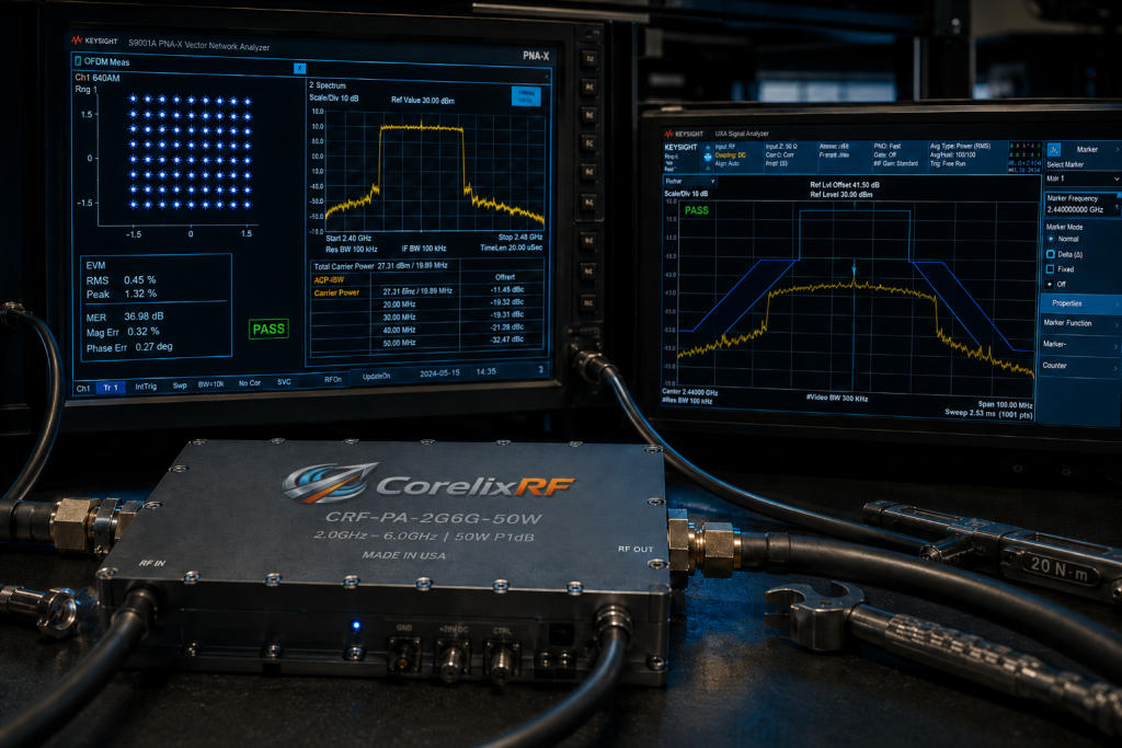
The fundamental physics dictate that theoretical design models must be relentlessly validated against physical hardware utilizing high-end laboratory test equipment. We quantify the success of our power-side termination filtering strategy by purposefully injecting synchronized multi-tone test signals into the CRF-PA-2G6G-50W while simultaneously superimposing severe, swept-frequency ripple voltages directly onto its primary direct current supply line. Using state-of-the-art vector network analyzers (VNAs) and high-dynamic-range spectrum analyzers, engineers measure the specific intermodulation distortion (IMD) products and precisely track the resulting RF EVM deterioration in real-time. A mathematically successful filter deployment will show zero measurable change in the thermal noise floor or the adjacent channel leakage ratio (ACLR) despite the extreme low-frequency perturbations forcibly applied to the bias port. We meticulously document the phase noise degradation under these highly aggressive test vectors, logically ensuring the amplifier maintains an ultra-low phase noise profile strictly necessary for high-order digital modulation schemes. This rigorous empirical validation proves absolutely that our custom hardware modifications successfully shield the RF signal path from the chaotic electrical realities of modern aircraft power grids.
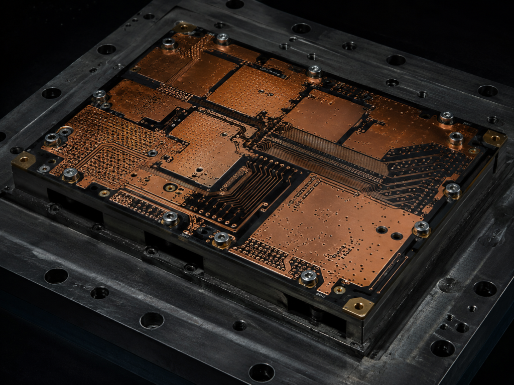
| Test Parameter | Input Test Condition | Allowable Hardware Deviation | Measurement Instrument |
| Ripple Rejection | 100mV P-P @ 500 kHz | < 0.1 dB Output Power Shift | Oscilloscope + VNA |
| EVM Stability | 64-QAM Burst Signal | < 0.5% EVM Increase | Vector Signal Analyzer |
| ACLR Impact | Two-Tone Carrier | No change in adjacent channel | Spectrum Analyzer |
| Thermal Cycle | -40°C to +85°C | Impedance shift < 5% | Environmental Chamber |
Conclusion
The integration of high-power amplification into airborne platforms requires an uncompromising approach to power conditioning. The physical reality proves that ignoring power distribution network filtering directly causes severe EVM degradation and generates destructive spurious emissions. By implementing highly rigid, localized decoupling networks, selecting thermally matched materials, and applying heavy component derating, the CRF-PA-2G6G-50W effectively isolates the microwave signal path from volatile system power buses. CorelixRF remains strictly committed to engineering truth, providing system integrators with hardware that mathematically guarantees continuous spectrum purity under the harshest physical conditions. Contact the CorelixRF engineering team today to request the official Data Sheet and integrate laboratory-verified reliability into your next avionics data link architecture.
FAQ
Q1: What happens if I use standard commercial capacitors for the PDN filter in an avionics data link?
Commercial capacitors feature brittle ceramic dielectrics that cannot withstand the mechanical vibration and extreme thermal cycling of aerospace environments. Under stress, they suffer micro-cracking, which drastically increases their equivalent series resistance (ESR) and completely destroys their ability to filter switching ripple, immediately leading to corrupted RF EVM.
Q2: How does CorelixRF manage the high thermal loads of the filtering inductors?
We manage these specific loads by utilizing advanced high-frequency laminates coupled with heavy copper internal layers. Furthermore, we place dedicated, laser-drilled thermal microvias directly beneath the high-dissipation filtering chokes to aggressively extract the heat directly to the mechanical baseplate, preventing thermal runaway.
Q3: Why is localized decoupling near the GaN transistor drain so critical for the CRF-PA-2G6G-50W?
Placing bypass capacitors fractions of a millimeter away from the active drain minimizes the parasitic series inductance of the copper traces. This lack of inductance physically allows the transistor to draw instantaneous high-current pulses required for broadband modulation without suffering localized voltage droop.
Q4: Can ordinary switching power supply ripple physically damage the RF amplifier?
Yes. Severe low-frequency ripple forces the active transistors to constantly operate outside their linear bias points. This generates excessive heat and massive intermodulation distortion, which over time can cause dielectric breakdown, thermal exhaustion, and the total physical destruction of the active semiconductor die.
Q5: How does impedance mismatch at the power terminal affect output power?
A high impedance mismatch severely reflects the transient energy required by the amplifier back into the power bus. This restricts the total instantaneous current available to the active devices, actively choking the transistor and drastically reducing the saturated output power capability across the operational bandwidth.