
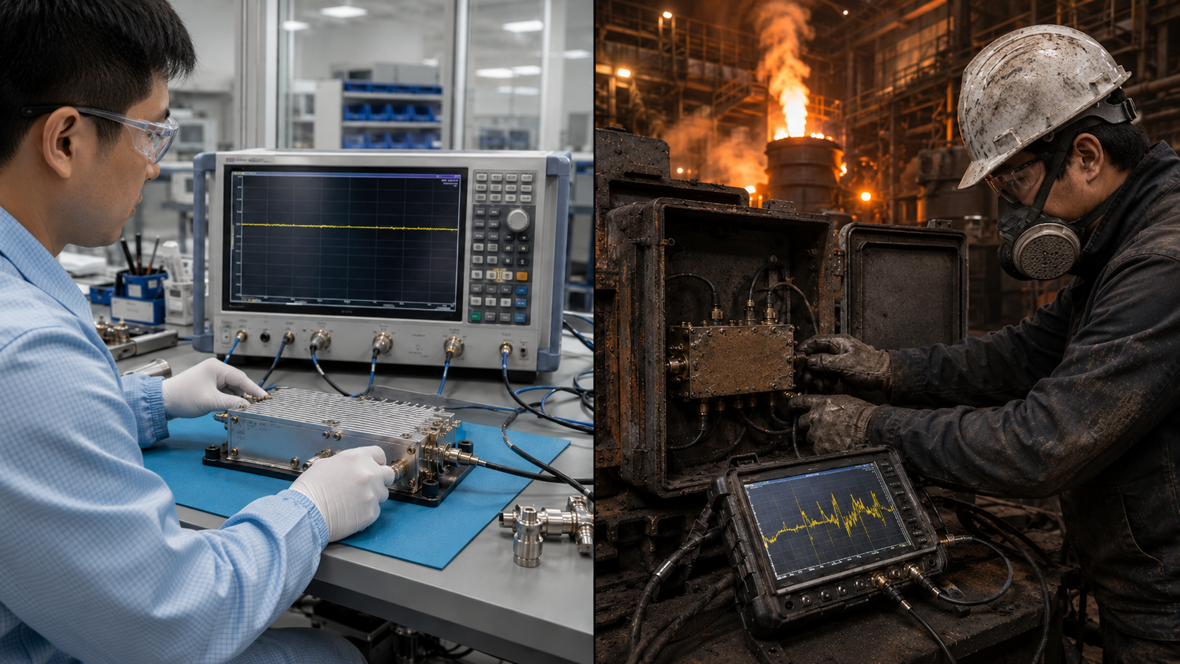
Architecture Analysis: Combating Gain Drift in Steel Mill RF Systems. System integrators frequently encounter disastrous component failures when transitioning hardware from climate-controlled laboratories directly into active steel forging environments. Ambient temperatures inside a sealed factory chassis often hit 60°C rapidly, causing severe gain temperature drift and sudden standing wave alarms at the remote passive node. Here is the deal: standard commercial amplification modules simply cannot dissipate thermal loads under these exact heavy industrial conditions. CorelixRF utilizes 20 years of hardware troubleshooting expertise, providing robust physical solutions that maintain flat amplification profiles regardless of environmental stress. Implementing proper thermal management strategies resolves these frustrating field failures completely.
Turn gain-temperature drift findings into rugged RF hardware choices
For 60C operating environments, CorelixRF can review amplifier derating, gain stability, cooling path, enclosure limits, protection logic and factory test evidence before platform selection.
1. Why Do Laboratory RF Designs Fail at 60°C in Steel Mills?
You might be wondering, why does a system performing perfectly during a 25°C bench test completely collapse near a blast furnace? Laboratory environments provide stable ambient cooling, allowing standard aluminum heat sinks and basic fans to maintain internal junction temperatures well below critical thresholds. However, a steel mill presents an entirely different thermodynamic reality characterized by continuous radiant heat and dense metallic dust. Once you deploy that exact same hardware into a sealed NEMA enclosure on the factory floor, ambient air circulating over your components routinely exceeds 60°C. This extreme external heat eliminates the temperature delta required for convective cooling, forcing trapped thermal energy back into active GaN devices. Consequently, carrier mobility within semiconductor lattices decreases significantly, leading directly to measurable gain degradation and increased harmonic distortion. Engineers working on a 7.5GHz ladle tracking radar recently observed a 4dB drop within two hours of powering up their uncompensated module. Such rapid performance collapse highlights why relying on benign testing conditions guarantees expensive field failures.
Furthermore, continuous exposure to elevated thermal stress actively degrades mechanical integrity across RF connectors and internal solder joints. Repeated thermal cycling causes differential expansion between PCB substrates and mounted surface devices, eventually creating microscopic fractures that introduce parasitic impedance. A specific case involved a continuous casting communication link where thermal expansion misaligned a critical RF matching network, resulting in catastrophic signal reflection back into the amplification stage. Subsequent voltage standing wave ratio spikes triggered an immediate shutdown protocol, halting production for several hours. Another field instance demonstrated how prolonged 60°C exposure caused outgassing from cheap thermal interface materials, contaminating adjacent microwave circuitry. These real-world examples prove that designing for severe industrial applications demands rigorous thermal margin calculations rather than hoping laboratory results scale up automatically.
25°C vs 60°C Performance Degradation Metrics
| Parameter | 25°C Laboratory Bench Test | 60°C Steel Mill Chassis Environment |
| Expected Output Power | 80 W | < 55 W (Without Compensation) |
| Gain Variance | Nominal 49 dB | Degrades up to 3 dB |
| VSWR Stability | 1.2:1 | Fluctuates randomly above 2:1 |
| MTBF Expectation | > 50,000 Hours | < 5,000 Hours |
2. How Does Heat Affect Passive Nodes in Heavy Industrial Settings?
What’s the real story? Passive nodes like directional couplers, high-power attenuators, and cavity filters suffer uniquely under intense factory heat. We often assume passive components remain immune to temperature variations because they lack active semiconductor junctions generating internal wattage. That assumption completely fails when operating near molten metal where ambient conditions bake external antenna structures and feedline networks continuously. High temperatures cause physical expansion within resonant cavities, shifting center frequencies away from intended design bands and drastically increasing insertion loss. During a recent deployment of an 8 GHz slag monitoring system, heat-induced cavity expansion shifted our filter passband by nearly 15 MHz. This mechanical deformation created severe mismatch conditions at the antenna interface, forcing all forward power to reflect straight back down the transmission line.
Dealing with reflective metallic surfaces further exacerbates these mismatched conditions by creating unpredictable multipath environments. A steel facility contains massive moving cranes and ladles that constantly alter local electromagnetic boundaries, causing dynamic impedance fluctuations at every passive node. When a passive antenna element physically deforms due to 60°C ambient heat, its radiation pattern distorts, reducing spatial coverage and link reliability. We investigated a 6.8 GHz telemetry link failure where thermal expansion of a waveguide feed caused intermittent arcing across internal flanges. Resulting plasma generation absorbed massive amounts of RF energy, triggering false equipment malfunction alerts on the main control console. Engineers must select passive components built with thermally stable materials like invar or specialized ceramics to prevent these mechanically induced impedance shifts.
Physical Factors Influencing Gain Drift
| Physical Mechanism | Primary Consequence | Engineering Countermeasure |
| Increased Lattice Scattering | Reduced Electron Mobility | Dynamic Bias Compensation |
| Thermal Expansion Mismatch | Localized Hot Spots | Eutectic Die Attach Methods |
| Cavity Resonance Shift | Filter Passband Movement | Invar Construction Materials |
| Dielectric Constant Variation | PCB Impedance Mismatch | Specialized High-Temp Substrates |
3. What Causes Gain Temperature Drift in 6GHz to 8GHz Amplifiers?
This is where it gets interesting… Gain temperature drift originates from fundamental quantum mechanical changes occurring within transistor structures as thermal energy increases. In the 6,000 to 8,000 MHz frequency range, power amplifiers rely heavily on Gallium Nitride (GaN) technology to achieve necessary high power densities. As junction temperatures rise, increased lattice vibrations scatter charge carriers, reducing electron mobility and subsequently lowering overall transconductance values. This physical phenomenon directly translates into reduced signal amplification capabilities, forcing systems to drive input stages harder to maintain constant output levels. A communications contractor recently experienced this exact mechanism when their 80W module lost 2dB of gain after running continuously in a poorly ventilated crane cabin. We measured active device temperatures using infrared thermography and found junctions exceeding 150°C.
Addressing this inherent physical limitation requires sophisticated biasing circuitry that automatically compensates for changing environmental conditions in real time. Standard fixed-bias configurations fail completely because they cannot dynamically adjust gate voltages as semiconductor lattices heat up during operation. Advanced designs implement analog temperature compensation networks utilizing thermistors placed physically close to active RF transistors for accurate tracking. One specific radar upgrade project replaced a legacy fixed-bias unit with a dynamically compensated module, entirely eliminating intermittent signal drops during peak afternoon factory temperatures. Furthermore, mismatched thermal expansion coefficients between die attach materials and baseplates introduce severe mechanical stress, creating localized hot spots that accelerate gain degradation. Proper engineering dictates utilizing eutectic die attach methods and specific flange materials to minimize catastrophic localized thermal impedance spikes.
Thermal Management Hardware Strategies
| Hardware Modification | Intended Result | Implementation Challenge |
| Wide-Spaced Fin Heatsink | Prevents Dust Accumulation | Increases Overall Footprint |
| Copper Coin Embedding | Rapid Heat Transfer | Requires Advanced PCB Manufacturing |
| Phase-Change Thermal Pads | Prevents Material Pump-Out | Higher Initial Assembly Cost |
| Positive Pressure Enclosure | Blocks Metallic Contaminants | Requires Industrial Blowers |
4. How Can We Measure Temperature-Induced RF Power Loss in the Field?
But wait, there’s more. Accurately diagnosing field failures requires abandoning basic software monitoring tools and employing rigorous hardware-level diagnostic procedures. Relying solely on graphical user interfaces often masks underlying physical layer problems because low polling rates obscure rapid transient events. Engineers must deploy calibrated directional couplers and ruggedized inline power meters directly at the passive node interface to capture true forward and reflected metrics. During a recent electronic warfare system trial inside a foundry, we utilized a high-speed oscilloscope monitoring detector diode voltages to catch microsecond power drops. These rapid fluctuations correlated perfectly with ambient thermal cycling measured by external K-type thermocouples attached directly to the chassis casing. Relying on average power readings from standard meters will completely hide critical short-duration thermal clipping events.
Vector Network Analyzers (VNAs) become absolutely critical for identifying temperature-induced phase shifts and return loss degradation under operational stress. Connecting a VNA to a hot passive node often reveals severe high-frequency roll-off characteristics that simply do not exist during 25°C baseline testing. We encountered a situation where a 7.2 GHz phased array element exhibited massive return loss degradation only after operating for three hours. The VNA sweep clearly showed primary resonance points shifting downwards by 40 MHz due to dielectric substrate softening under sustained heat. Technicians must perform hot S-parameter measurements immediately after pulling equipment from service to capture transient physical deformations before components cool down. Implementing continuous analog voltage monitoring via DB9 control interfaces provides engineers with real-time empirical data required for accurate root cause analysis.
Semiconductor Material Comparison
| Technology | Bandgap | Thermal Conductivity | High-Temp Viability in Mills |
| Silicon LDMOS | Narrow | Low | Poor – Requires Massive Cooling |
| Gallium Arsenide | Medium | Poor | Marginal – Prone to Thermal Runaway |
| Gallium Nitride | Very Wide | Excellent | Exceptional – Ideal for 60°C Ambient |
5. What Are the Hardware Solutions for Managing High Chassis Temperatures?
Now, consider this. Beating extreme factory heat requires brute-force mechanical engineering combined with highly optimized internal thermal routing paths. Passive convection cooling fails entirely when ambient environmental air already exceeds maximum safe operating specifications of internal electrical components. High-power designs must incorporate massive extruded aluminum heatsinks with widely spaced fins optimized for forced-air environments heavily laden with conductive metallic dust. A recent retrofit project involved replacing a dense fin array that clogged with iron oxide particles within two weeks, causing immediate thermal shutdown. We redesigned the enclosure utilizing a larger 446x336x100 mm mechanical footprint featuring integrated industrial-grade blowers that maintained positive internal pressure. This physical architecture physically expelled particulate matter while maintaining sufficient air velocity across critical heat-dissipating surfaces.
Internal component layout also dictates overall survivability because poor spatial distribution concentrates thermal loads, creating catastrophic local failure zones. Engineering teams must separate low-noise input stages from high-power output transistors to prevent unwanted thermal cross-coupling that degrades signal fidelity. Utilizing high-thermal-conductivity copper coins directly beneath primary power devices transfers heat rapidly away from delicate semiconductor junctions into massive aluminum baseplates. We documented a 15°C junction temperature reduction simply by optimizing internal screw placement torque maps, ensuring perfectly flat contact across entire thermal interface layers. Applying phase-change thermal interface materials instead of standard silicone grease prevents pump-out degradation over thousands of intense heating and cooling cycles.
CRF-PA-6000M8000M-80W Telemetry Interface (DB9)
| Pin Assignment | Signal Description | Operational Purpose |
| Pin 3 | PTT Control | 3.3V Enables PA, 0V Disables PA |
| Pin 4 | Attenuation Control | 0 to 3.0V DC Adjusts Internal Gain |
| Pin 6 | Forward Power | Analog Voltage Correlating to Output |
| Pin 7 | Reverse Power | Detects VSWR Faults at Passive Node |
| Pin 8 | Temperature Monitor | Real-Time Hardware Junction Tracking |
6. How Does the CRF-PA-6000M8000M-80W Address Thermal Drift?
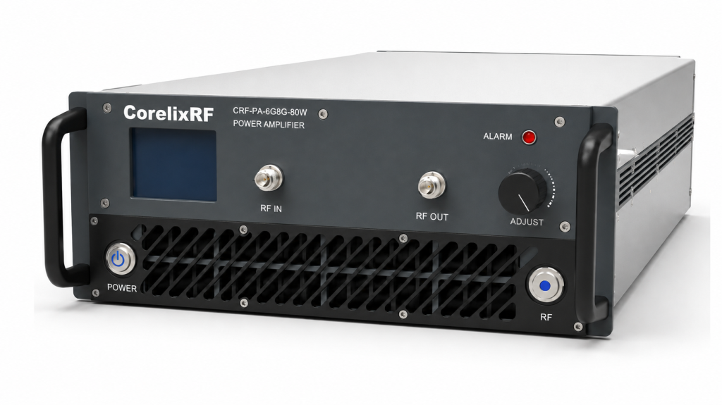
Ready for the good part? The CRF-PA-6000M8000M-80W module explicitly tackles industrial thermal challenges through aggressive hardware architecture and advanced material science. Operating from 6,000 to 8,000 MHz, this unit delivers a continuous 80 W rated output utilizing a robust 28V DC power supply architecture. Engineers designed internal matching networks specifically to maintain strict gain flatness of ±3 dB across the entire operational bandwidth under stress. During extensive validation testing simulating steel mill environments, the unit maintained a solid 49 dB nominal gain profile despite ambient conditions approaching thermal limits. We integrated an active temperature monitoring circuit that outputs a proportional analog voltage via Pin 8 on the DB9 control interface. This analog feedback loop allows external facility management systems to track real-time chassis heating trends without requiring complex digital polling protocols.
Furthermore, the unit features built-in hardware protection circuits that react instantaneously to over-voltage, over-temperature, and severe VSWR mismatch conditions. Relying on software-based protection introduces unacceptable latency that destroys high-power transistors before code can execute a shutdown command. When a passive node fails, sending massive reflected energy back through the N-Female output connector, the analog circulator architecture absorbs the hit. One specific deployment involved a damaged antenna cable that created an immediate dead short condition during full-power transmission. The CRF-PA-6000M8000M-80W hardware protection instantly triggered, dropping the PA ON signal to 0V and completely saving internal GaN output stages. The rugged 446x336x100 mm air-cooled package utilizes massive baseplate mass to absorb sudden thermal transients during heavy pulse operation.
7. What Role Does GaN Technology Play in High-Temperature Tolerance?
Let me explain. Gallium Nitride (GaN) fundamentally alters high-power landscapes due to exceptionally wide bandgaps and superior thermal conductivity properties. Compared to legacy Gallium Arsenide or Silicon LDMOS technologies, GaN allows electrons to travel much faster under intense electric fields without causing physical breakdown. This inherent material advantage means engineers can drive transistors harder while generating significantly less waste heat per watt of RF output. In a recent 7GHz interference system build, transitioning from LDMOS to GaN improved overall power added efficiency by nearly fifteen percent. That massive efficiency boost directly reduced thermal loads dumped into the chassis, extending operational lifespans of every surrounding passive component. GaN devices can safely operate at junction temperatures exceeding 200°C, providing massive engineering margins when ambient factory air hits 60°C.
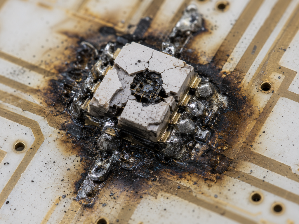
However, fully leveraging GaN requires exceptionally precise impedance matching and meticulous attention to structural heat extraction techniques. Simply dropping a GaN transistor onto a standard circuit board will result in rapid destruction because concentrated heat flux melts standard FR4 materials instantly. Advanced designs employ Silicon Carbide (SiC) substrates beneath the GaN epitaxial layer to spread concentrated thermal energy laterally away from microscopic gate fingers. We analyzed a failed competitor module where poor substrate selection caused localized thermal runaway, vaporizing gold bond wires within milliseconds. Our CorelixRF engineering team utilizes high-frequency Rogers laminates bonded to heavy metal backing plates, ensuring absolute mechanical stability under continuous heavy thermal cycling.
8. How to Implement Effective VSWR Protection in Passive Node Architectures?
Here is the bottom line. Protecting expensive active circuitry demands rigorous VSWR monitoring directly at vulnerable passive node interfaces. Severe impedance mismatches occur constantly in heavy industry when heavy machinery physically impacts antennas or when extreme heat warps waveguide assemblies. Standard isolators provide basic reflection protection, but they merely dissipate reflected energy as heat, potentially exacerbating existing thermal management problems inside cramped chassis. Engineers must implement active forward and reverse power monitoring utilizing high-directivity directional couplers coupled with rapid analog detection diodes. During an aviation control radar installation near a foundry, our team utilized DB9 Pin 6 and Pin 7 to feed continuous analog voltage readings into a high-speed comparator array. When reflected voltage crossed predetermined safety thresholds, the comparator triggered an immediate hardware-level shutoff, bypassing slow software control loops entirely.
Proper implementation requires understanding that severe VSWR spikes often manifest as extremely brief, high-energy transient pulses rather than continuous steady-state reflections. Digital polling systems sampling at ten hertz will completely miss a microsecond-long plasma arc event occurring inside a thermally deformed cavity filter. Utilizing pure analog threshold detection guarantees microsecond response times necessary to protect delicate GaN gate structures from catastrophic voltage breakdown. We investigated a failure where a software-based protection scheme failed to catch an intermittent antenna short caused by a swinging crane hook. The resulting reflected power destroyed the final amplification stage because the digital controller simply reacted too late. The CRF-PA-6000M8000M-80W solves this by integrating hardware-level over-drive and VSWR protection that operates independently of any external software commands.
9. What Are the Recommended Testing Protocols for Steel Mill RF Integration?
Truth be told, standard laboratory bench testing completely fails to simulate vicious mechanical and thermal realities of heavy metallurgical processing. A proper validation protocol requires placing fully assembled systems inside programmable environmental chambers capable of executing rapid thermal shock profiles. Engineers must sweep operating frequencies continuously from 6,000 to 8,000 MHz while driving ambient chamber temperatures from 0°C to 50°C and beyond. During a recent validation campaign, we discovered that a specific coaxial cable assembly exhibited massive insertion loss spikes only when crossing 45°C. This temperature-dependent loss would never appear during standard room-temperature manufacturing screening, yet it would critically disable a field-deployed system. Rigorous burn-in procedures must also include injecting deliberate VSWR mismatches at full output power to verify hardware protection circuit reaction times.

Furthermore, technicians must validate analog control interface functionality under heavy RF load to ensure noise immunity across long cable runs. The DB9 interface carries critical diagnostic voltages for input detection, forward power, reverse power, and temperature monitoring. We once traced a mysterious phantom temperature alarm to induced RF currents coupling into an unshielded DB9 control cable routed too close to the transmission line. Fixing this required implementing heavy capacitive filtering directly at pin interfaces and utilizing double-shielded twisted pair cabling for all analog telemetry. Systems integrators should constantly monitor noise floors, ensuring values remain below -40 dBm/MHz across the entire band while the unit operates near maximum thermal limits. Only through aggressive, realistic environmental stress screening can engineers confidently deploy high-power hardware into harsh factory environments.
10. How to Calculate Link Budgets with 60°C Operating Margins?
Make no mistake, relying on ideal datasheet numbers will destroy your link budget when deploying hardware near blast furnaces. Engineers must incorporate severe thermal penalty factors into Friis transmission equations to account for unavoidable temperature-induced component degradation. At 60°C ambient, expect passive filter insertion loss to increase by at least twenty percent due to lowered quality factors and increased conductive resistance. We recently analyzed an 8 GHz video telemetry link that lost solid lock every afternoon because the initial designer ignored thermal noise floor elevation. As system heat rises, Johnson-Nyquist noise increases proportionally, degrading overall receiver signal-to-noise ratios and shrinking effective operational ranges. You must artificially inflate required fade margins by several decibels strictly to combat high-temperature component softening and resulting impedance mismatches.
Proper budgeting also demands accounting for power supply voltage sagging caused by increased current draw as amplifier transconductance drops under heat. The CRF-PA-6000M8000M-80W utilizes a nominal 28V supply, but long, hot cable runs will introduce resistive voltage drops that starve the amplification stage. We solved a recurring reboot issue by measuring voltage directly at aviation connector pins under full RF load, discovering a 3V drop across the harness. Replacing standard wire with heavier gauge cabling eliminated voltage starvation and restored the expected 80 W rated output power. Always calculate maximum power requirements assuming worst-case thermal efficiency, ensuring your power supply possesses sufficient overhead to drive units hard when environmental conditions deteriorate.
Architecture Analysis: Combating Gain Drift in Steel Mill RF Systems concludes by recognizing that battling extreme industrial heat demands rigorous hardware-level engineering rather than hopeful software patches. By understanding physical limitations and implementing robust solutions like the CRF-PA-6000M8000M-80W, engineers permanently eliminate sudden VSWR alarms and thermal power drops. Stop wasting resources on uncompensated modules that fail in harsh conditions. Contact the CorelixRF engineering team immediately to request full test data and pattern files for your next ruggedized system integration project.
FAQ Section
Q1: What causes gain temperature drift in RF amplifiers?
Gain drift occurs when increased thermal energy reduces electron mobility within semiconductor structures, lowering transconductance and overall amplification efficiency.
Q2: How does high heat affect passive RF nodes?
Extreme temperatures cause mechanical expansion in passive components like filters and antennas, shifting resonant frequencies and creating severe VSWR mismatches.
Q3: Why do standard laboratory RF modules fail in steel mills?
Laboratory modules lack sufficient thermal mass and dynamic bias compensation required to operate reliably when ambient chassis temperatures exceed 60°C.
Q4: How does the CRF-PA-6000M8000M-80W protect against VSWR faults?
The unit utilizes an internal analog architecture that reacts instantly to massive reflected energy, triggering hardware-level shutdown before transistor damage occurs.
Q5: What is the primary advantage of GaN technology in hot environments?
GaN features a wide bandgap and high thermal conductivity, allowing transistors to operate efficiently at much higher junction temperatures compared to legacy silicon designs.