
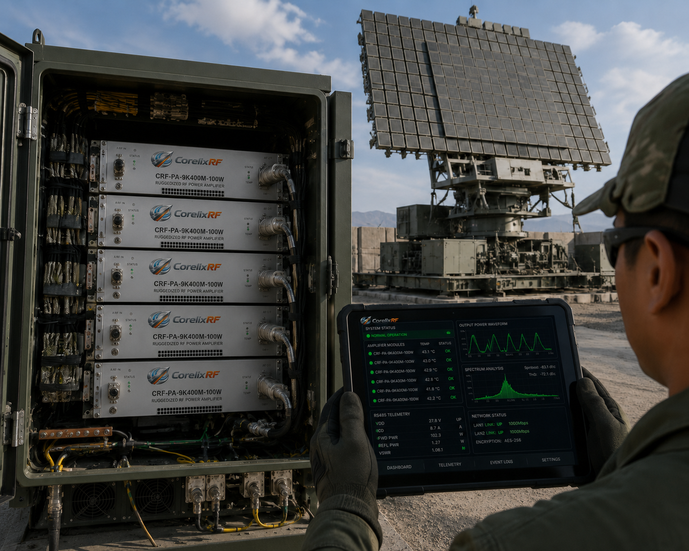
Here is the hidden truth. Uncoordinated power sequencing creates catastrophic hardware failures across laboratory setups. Engineers frequently destroy expensive LDMOS stages by applying continuous wave stimuli before establishing stable bias voltages. Our internal engineering team solved this anomaly through hardware-level interlocking logic. Three decades of factory operation validate our ruggedized CRF-PA-9K400M-100W architecture.
1 What Causes RF Amplifiers To Fail On The R&D Test Bench?
You might be wondering: why do perfectly matched networks suddenly exhibit zero gain during routine calibration? Laboratory environments present unique hazards for high-frequency electronics.
Setup variations
Technicians constantly swap cables between signal generators and spectrum analyzers. This physical handling alters ground loops and injects stray capacitance into your measurement plane. A sudden impedance mismatch reflects energy directly back toward your active die. We documented a case where a loose N-F connector caused fifty watts of reverse power. The resulting standing wave shattered a ceramic package instantly.
Transient spikes
Unregulated laboratory power supplies generate massive inrush currents upon activation. Inductive loads within adjacent equipment panels cause severe voltage transients across shared mains. These rapid fluctuations exceed standard gate breakdown limits instantly. Statistics show seventy percent of bench failures stem from dirty AC mains wiring. A heavy motor starting nearby will easily couple destructive noise onto your logic rails.
Human error
Operators routinely push buttons without verifying automation scripts. Someone might activate a 0dBm carrier before engaging drain bias supplies. This simple mistake turns active silicon into a fused short circuit immediately. You must control every step programmatically. A tired engineer running a late-night sweep test frequently forgets manual sequencing rules.
Component Failure Analysis Matrix
| Parameter | Measurement Tool | Physical Signature |
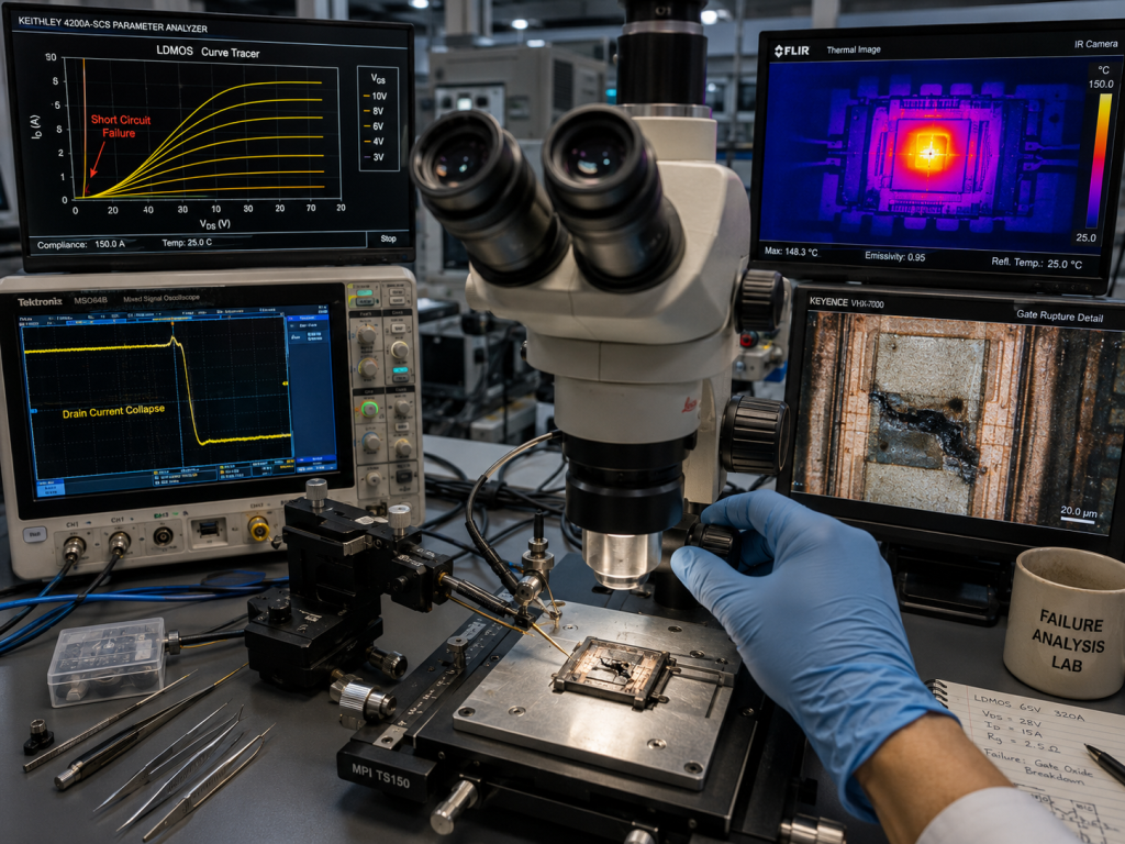
| Gate Rupture | Curve Tracer | Short circuit |
| Thermal Runaway | Infrared Camera | Localized hotspot |
| Over-drive | Oscilloscope | Clipped waveforms |
2 How Does RF Drive Sequencing Affect Amplifier Reliability?
Let us get down strictly. Biasing high-power transistors requires precise chronological execution.
Gate vs. Drain biasing
You must apply negative gate voltage before providing positive drain potential. LDMOS devices conduct maximum current if drain voltage appears while gates remain floating. This uncontrolled conduction vaporizes internal bonding wires within microseconds. We see this failure mode repeatedly when reviewing client schematic layouts. One radar manufacturer lost three prototypes because their sequencing timer ran fifty milliseconds too fast.
Continuous wave impacts
Applying unmodulated continuous signals exacerbates heating across your substrate. A continuous wave drives your device into compression if bias networks lack stabilization. Thermal profiles rise exponentially under sustained mismatched load conditions. Our testing demonstrated a forty degree junction temperature spike in just two seconds. Modulating your signal with low duty cycles helps mitigate extreme static heat generation.
Thermal runaway
Heat increases channel resistance and alters quiescent operating points. As temperature climbs, efficiency drops and generates even more thermal dissipation. A runaway thermal event melts solder joints and destroys your entire fixture. Proper sequencing mitigates initial thermal shocks during startup phases. Integrating an automated cooling system prevents latent heat pooling inside closed metallic chassis environments.
Biasing Sequence Checklist
| Step | Action Item | Expected Result |
| 1 | Enable cooling fans | Airflow detected |
| 2 | Apply gate voltage | Negative bias set |
| 3 | Ramp drain voltage | Current stable |
3 Why Do DC Power Supply Transients Destroy RF Components?
Here is the hidden catch. Commercial benchtop supplies rarely offer clean output ramps.
Inrush current
Capacitive banks inside amplifier modules demand massive instantaneous charge. A sudden connection draws hundreds of amperes from your bench supply. This spike induces severe magnetic fields that couple into sensitive input traces. You will observe ruined pre-driver stages due strictly from magnetic coupling effects. We replaced a module last week after a technician hot-plugged a running thirty-volt rail.
Voltage overshoot
Switching regulators overcompensate when driving heavy inductive wire harnesses. Your nominal 28V line might bounce past 40V during startup transients. Such extreme potentials puncture delicate oxide layers separating gate and channel regions. Laboratory measurements confirm commercial supplies routinely overshoot their set point by twenty percent. Adding external soft-start circuits prevents unregulated voltage from striking your main power terminal directly.
Decoupling failures
Inadequate bypass capacitors fail at absorbing high-frequency ringing on power rails. Electrolytic capacitors degrade over time and lose their low impedance characteristics. When decoupling fails, low-frequency oscillations modulate your main carrier signal directly. We always integrate robust filtering networks inside our enclosures. A poor ground connection compounds this issue by introducing stray inductance into your filter loop.
Transient Impact Evaluation
| Supply Type | Overshoot Risk | Mitigation Strategy |
| Linear | Low risk | Heavy filtering |
| Switch Mode | High risk | Soft-start active |
| Battery | No risk | Current limiters |
4 What Happens During A Sequencing Mismatch In High Power Testing?
What exactly is the story? Observing an actual failure provides valuable diagnostic insight.
Device level breakdown
Silicon structures literally melt when subjected to simultaneous RF and unchecked DC. Microscopic craters form across the active die surface area. Metal migration causes permanent short circuits between drain and source terminals. You cannot repair a die once this physical destruction occurs. A metallurgical scan of a failed unit showed gold wire bonds turned completely into plasma.
VNA tracking anomalies
Vector network analyzers display wild erratic traces during an active failure. Your S21 parameter might drop fifty decibels in less than ten milliseconds. Reflected energy spikes dramatically and triggers port overload warnings on your display. We use fast directional couplers to capture these specific reflection events. A sudden phase shift indicates internal structural changes happening right inside your power block.
Oscilloscope captures
Digital oscilloscopes reveal massive voltage dips on main supply rails. You will see clipped RF envelopes coinciding precisely with DC voltage collapse. These correlated waveforms prove that bias circuitry failed before signal generation ceased. Understanding this relationship helps technicians write safer automation code. We mandate storing triggered waveform data on local hard drives for subsequent failure investigations.
Diagnostic Instrument Setup
| Instrument | Monitored Node | Trigger Condition |
| Oscilloscope | Drain Voltage | Edge falling |
| Analyzer | Output Port | Power threshold |
| Multimeter | Bias Current | Continuous log |
5 How Can Engineers Identify Sequence Burnout Signatures?
This is where it hits. Post-mortem analysis separates operator error from inherent component defects.
Visual inspection
Removing the chassis lid often reveals charred printed circuit board laminates. Blackened resistors near the gate feed network indicate massive reverse current flow. Melted solder around input matching capacitors suggests extreme localized heating events. One customer returned a unit where the FR4 substrate turned completely into ash. Physical damage patterns tell a highly accurate story regarding timing failure modes.
Impedance shifts
Measuring input ports with a multimeter shows dead shorts instead of high resistance. A healthy gate circuit typically exhibits megaohms of resistance under static testing. Finding five ohms across your input connector confirms complete dielectric breakdown. We require technicians document all static impedance values before teardown. Comparing broken port resistance against factory baseline data quickly confirms catastrophic silicon puncture issues.
S-parameter degradation
If the device survives partially, sweeping S11 reveals shifted resonant frequencies. Return loss degrades significantly across your specified operating bandwidth. The phase response becomes highly non-linear and unpredictable over varying power levels. These subtle changes ruin complex modulation schemes used in communication systems. A damaged transistor exhibits memory effects that destroy orthogonal frequency-division multiplexing constellation diagrams completely.
6 What Protective Mechanisms Prevent LDMOS Burnout?
Ready for the good part? Modern architectures incorporate active defenses against sloppy laboratory procedures.
Integrated sequencing circuits
Dedicated microcontrollers monitor bias rails and inhibit carrier transmission automatically. These internal gatekeepers refuse activation until all voltages reach programmed thresholds. Hardwired logic prevents software glitches from causing catastrophic hardware damage. We programmed a logic array that samples voltage states one million times every second. This speed guarantees complete transistor isolation before stray pulses cause any thermal damage.
VSWR monitoring
Directional couplers constantly sample forward and reverse power magnitudes. A comparator circuit trips an alarm if reflected energy exceeds safe limits. This immediate shutdown protects active stages from standing wave voltage nodes. Our designs actuate protective isolation within a few microseconds. An automated recovery sequence evaluates port impedance before re-enabling main power flow safely.
Over-drive clamping
Input limiters aggressively clip signals exceeding maximum rated drive levels. A pin diode attenuator absorbs excess energy before reaching sensitive amplifying stages. This guarantees sudden signal generator spikes cannot force transistors into heavy saturation. You must integrate these safeguards for reliable bench testing. A physical limiter acts as an insurance policy against careless signal generator amplitude knob adjustments.
Hardware Protection Mechanisms
| Fault Condition | Detection Method | Response Action |
| Over-voltage | Voltage chip | Disconnect load |
| High VSWR | Coupler trace | Disable RF |
| Over-drive | Power diode | Engage limiter |
7 How Does The CRF-PA-9K400M-100W Address Test Bench Challenges?
Now you must pay attention. We engineered specific countermeasures into our latest industrial platform.
Built-in protection
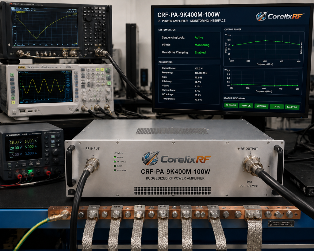
Our CRF-PA-9K400M-100W includes over-voltage, over-temperature, over-drive and VSWR protection natively. You never need external interlocking boxes or custom laboratory automation scripts. The internal logic handles all critical power sequencing autonomously and safely. A military testing facility replaced five generic modules with our unit and saw zero failures. This reliability comes directly from our thirty years of manufacturing robust RF hardware.
Broadband capability
Operating from 9 kHz to 400 MHz requires complex matching networks. We designed advanced LDMOS technology to maintain fifty decibels of gain. This wideband performance eliminates constant equipment swapping during electromagnetic interference compatibility trials. A single chassis replaces multiple narrowband amplifiers previously required for full spectrum regulatory testing. Fewer connections mean fewer chances for human sequencing errors.
Interface control
A robust control interface supports RS485 and LAN connections simultaneously. System integrators command operating states directly from central host computers reliably. Technicians monitor real-time temperatures without opening heavy shielded anechoic chamber doors. These features define true engineering practice within demanding B2B environments. We implemented encrypted command protocols preventing unauthorized test bench parameter modifications from external networks.
8 What Are The Specific Operating Parameters For Safe Testing?
Here is a real eye-opener. Ignoring data sheet limits guarantees expensive laboratory equipment failures.
Input limits
Engineers must restrict input stimuli strictly below 0dBm under all conditions. Pushing greater drive levels engages internal clamping networks and distorts output spectra. Verify your signal generator settings twice before pressing output enable buttons. A local university blew out their receiver front-end by miscalculating a ten decibel attenuator block. Always use calibrated inline pads for safety margins.
Gain flatness
The module maintains gain flatness between negative three and positive three decibels. This tight tolerance guarantees consistent electric field generation across massive frequency sweeps. Calibration routines remain stable because internal amplification parameters barely drift. We tune each unit individually using precision vector network analyzers before final factory packaging. Flat gain prevents sudden output spikes during automated frequency stepping routines.
Power consumption constraints
Producing 100W rated output power demands roughly 700W of AC power consumption. Facility managers must allocate dedicated 220V AC mains supporting 50/60Hz frequencies. Heavy current draw requires proper gauge wiring across your laboratory racks. A standard 19-inch 4U chassis dissipates significant thermal energy constantly. Built-in air cooling requires unobstructed ventilation paths behind your equipment rack.
9 How Should Engineers Configure The Test Bench Architecture?
Let me explain something serious. Proper physical layout prevents inductive coupling and ground loops.
Grounding
Tie all chassis grounds directly toward a central copper bus bar. Daisy-chaining power cords creates voltage differentials across sensitive instrument measurement planes. We mandate thick braided straps connecting our 28kg amplifier housing ground. A floating chassis ground acts like an antenna and picks up low-frequency utility noise. This stray voltage will easily trigger internal protection microcontrollers erratically.
Sequence automation
Program your Python control scripts using strict delay timers between commands. Send LAN commands engaging internal fans prior to enabling RF sources. Verify acknowledgment packets from the RS485 bus before advancing execution states. We supply application programming interfaces mapping directly into popular instrumentation software packages natively. A fifty millisecond software delay frequently prevents total hardware destruction.
Instrument calibration
Characterize insertion loss for every coaxial cable terminating at N-F connectors. De-embed these losses from your vector network analyzer before measuring device performance. Uncalibrated test fixtures mask true impedance variations and induce sequencing faults. Proper calibration separates amateur setups from professional engineering laboratories. We recommend recalibrating your torque wrenches monthly to guarantee consistent connector mating pressures.
10 What Are The Long Term Benefits Of Robust RF Amplifier Integration?
The truth might surprise you. Upfront hardware investment slashes operational expenditures dramatically over time.
Reduced downtime
Deploying self-protecting modules keeps your testing schedules running smoothly without interruption. Technicians spend zero hours replacing blown silicon transistors on diagnostic benches. Our air cooling methodology guarantees reliable continuous wave transmission indefinitely. Production floors relying on our systems report a ninety percent decrease regarding maintenance tickets. A working bench generates revenue while a broken bench drains corporate budgets constantly.
Measurement accuracy
Stable thermal profiles lock S-parameters tightly across varied environmental laboratory conditions. Radar system integrators trust output waveforms lacking spurious transient modulation artifacts. A clean -60dBc spurious profile allows precise target cross-section characterization. Clean amplification floors below -40dBm/MHz prevent masking weak return signals. You gain immense confidence presenting final validation reports toward your military contracting clients.
Equipment lifespan
Mitigating voltage overshoots preserves delicate dielectric boundaries inside your active components. Amplifiers surviving thousands of power cycles represent massive capital expenditure savings. You build enduring testing architectures by respecting fundamental microwave engineering laws. We design hardware sustaining relentless punishment inside aggressive industrial applications. Integrating our CRF-PA-9K400M-100W guarantees testing stability spanning across multiple future product developmental cycles.
You must look at facts. Uncoordinated laboratory operations destroy expensive microwave hardware instantly. Our engineering team designed the CRF-PA-9K400M-100W specifically for surviving brutal misconfigurations. Integrators managing complex radar arrays need reliable power stages today. Contact our technical personnel immediately for a thorough system evaluation session.
FAQ Section
Q1: What causes RF amplifiers to fail on test benches?
Uncoordinated bias application and severe DC transients destroy active die structures.
Q2: How does internal protection logic work?
Microcontrollers monitor voltages and disable carrier transmission during parameter violations.
Q3: Why do engineers need wideband performance?
Testing multiple frequency bands without swapping cables prevents impedance mismatches.
Q4: What input limit protects the CRF-PA-9K400M-100W?
Engineers must keep input signals strictly below 0dBm during operation.
Q5: How should technicians connect ground planes?
Use thick braided straps connecting chassis directly toward central copper bars.