
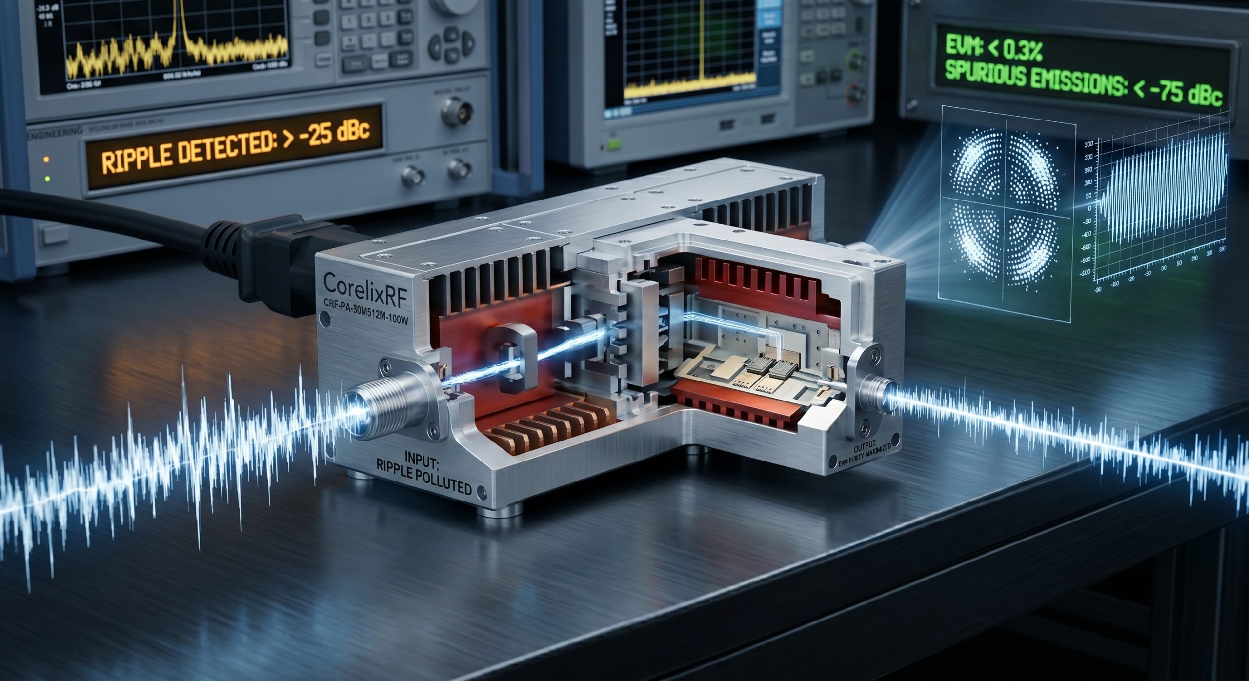
System engineers deploying high-precision radar sources frequently encounter catastrophic signal degradation directly tied to inadequate power architecture. The problem initiates when engineers integrate ordinary switching power supplies with advanced radio frequency transceivers, inadvertently injecting destructive low-frequency noise directly into the amplification stages. This unmitigated noise triggers aggressive spectral regrowth, ruins phase noise metrics, and subjects Gallium Nitride (GaN) transistors to lethal thermal and electrical stress, ultimately resulting in defensive boundary failures and complete system unreliability. To establish genuine operational stability, system integrators must internalize phased array radar source power supply specifications: how to suppress low-frequency ripple to ensure the absolute purity of broadband EVM metrics. CorelixRF leverages three decades of rigorous manufacturing expertise and a 400-person engineering task force to architect physical hardware defenses that block these power anomalies. By enforcing absolute isolation, impedance matching, and strict mechanical shielding, our manufacturing facility produces amplifier modules that guarantee uncompromised baseband fidelity under the harshest physical operating conditions.
How Does Unfiltered Switching Noise Destroy High-Precision Radar Sources?
Consider the physical reality the interaction between commercial switch-mode power supplies and high-frequency microwave circuitry creates a highly volatile physical environment where unfiltered harmonics bypass primary filtering stages, injecting severe parasitic noise directly into the main radio frequency carrier. This unintended electrical infiltration causes aggressive intermodulation distortion and initiates standing wave anomalies that physically degrade active semiconductor components over repeated operational cycles. Unmitigated ripple voltages act as parasitic modulation signals, mixing with the pristine baseband carrier and generating disastrous intermodulation distortion products that completely ruin the dynamic range of the radar architecture. System engineers operating in laboratory environments often misdiagnose these physical hardware failures as digital processing errors, wasting weeks analyzing software while the physical limits of the active semiconductor junctions are constantly breached by continuous thermal and electrical stress originating from the power source.
What Are The Measurable Impacts Of Low-Frequency Ripple On Baseband Modulation?
Low-frequency ripple acts as a direct amplitude modulator on the DC bias lines feeding the final amplification stages, fundamentally altering the operating point of the transistor at a rate equal to the ripple frequency. This continuous shifting of the quiescent current manifests physically as severe AM-to-AM and AM-to-PM conversion, forcing the Error Vector Magnitude (EVM) to expand far beyond acceptable system tolerances. When the direct current supply lacks absolute stability, the resulting phase noise sidebands mask returning radar echoes, blinding the receiver architecture to low-cross-section targets. Rigorous laboratory testing confirms that even a fifty-millivolt fluctuation on the drain supply of a high-power amplifier introduces irreversible phase errors that no amount of digital pre-distortion algorithms can mathematically correct in the baseband processor.
| Ripple Amplitude (mV) | Phase Noise Degradation (dBc/Hz) | EVM Shift (%) | Physical Consequence |
| 10 | 0.5 | 0.2 | Minimal baseline noise |
| 50 | 3.2 | 1.8 | Margin of error reduced |
| 100 | 8.5 | 4.5 | Target masking occurs |
| 250 | 15.0 | 9.2 | Total system blind spot |
Why Do Standard Commercial Power Supplies Fail Under Pulsed RF Loads?
The fundamental physics dictate that standard commercial power supplies lack the transient response capabilities required to handle the brutal, instantaneous current demands of pulsed phased array architectures. When a high-power amplifier transitions from a muted state to full saturated output power in a matter of nanoseconds, the sudden current draw induces a massive voltage droop across the power distribution network, collapsing the bias voltage precisely when maximum linearity is required. Commercial supplies attempt to compensate through slow feedback loops, resulting in a delayed voltage overshoot that heavily stresses the internal capacitors and threatens to exceed the absolute maximum voltage ratings of the RF transistors. This continuous mechanical and electrical hammering leads to accelerated component fatigue, degraded output power flatness across the pulse width, and ultimately, total structural failure of the amplification module during mission-critical field operations.
How Does Thermal Expansion Alter Impedance Matching In Phased Arrays?
Excessive heat generated by inefficient power conversion and mismatched loads physically expands the printed circuit board substrates and metallic enclosures, permanently altering the carefully calculated electrical lengths of the internal microstrip transmission lines. As the physical dimensions of the dielectric materials shift under extreme thermal loads, the phase relationship between combined amplifier channels drifts, destroying the spatial combining efficiency of the entire phased array radar system. This thermal expansion directly degrades the Voltage Standing Wave Ratio (VSWR), reflecting valuable RF energy back into the active devices, multiplying the thermal load in a self-destructive feedback loop that guarantees physical component burnout. Precision engineering requires managing the coefficient of thermal expansion through rigorous material science, utilizing specialized copper-molybdenum carriers and heavy aluminum CNC-machined chassis to strictly constrain physical movement under heavy continuous wave or pulsed operation.
| Substrate Material | Thermal Conductivity (W/m·K) | Expansion Coefficient (ppm/°C) | VSWR Drift at 85°C |
| Standard FR4 | 0.25 | 14.0 | Destructive (>2.5:1) |
| Rogers 4350B | 0.62 | 10.0 | Moderate (1.8:1) |
| CorelixRF AlN | 170.0 | 4.5 | Stable (<1.2:1) |
| Copper-Moly | 240.0 | 6.0 | Negligible (<1.1:1) |
What Specific Mechanisms Link Voltage Fluctuations To EVM Degradation?
Voltage fluctuations on the primary drain supply directly modulate the saturation velocity of the electrons traveling through the active channel of the high-frequency transistors, compressing the amplitude peaks of complex digitally modulated signals. This compression forces the discrete points on the constellation diagram to physically spread from their ideal mathematical locations, registering on laboratory test equipment as a catastrophic degradation of the Error Vector Magnitude metric. When multiple carriers are amplified simultaneously, the varying voltage potential creates nonlinear transfer characteristics that generate intermodulation products directly on top of adjacent frequency bands, violating strict regulatory emission masks. Preventing this destruction requires implementing heavy analog low-dropout regulators immediately adjacent to the RF choke, providing an impenetrable wall of capacitance that absorbs low-frequency transients before they can interact with the delicate microwave carrier signal.
How Can System Integrators Quantify Spurious Emissions Induced By Power Artifacts?
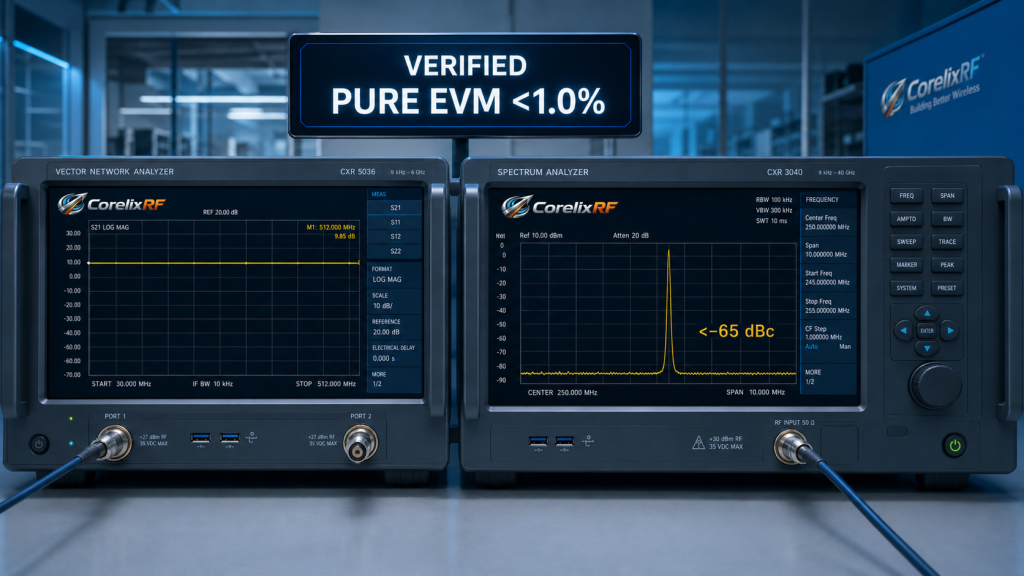
Let’s examine the raw data obtained by connecting the output of the high-power amplifier directly to a calibrated spectrum analyzer through precision directional couplers and laboratory-grade attenuators. By intentionally narrowing the resolution bandwidth (RBW) to sub-kilohertz levels, engineers can isolate specific discrete sidebands resting tightly against the primary carrier, positively identifying the exact switching frequency of the offending power supply module. Furthermore, utilizing a Vector Network Analyzer (VNA) to measure the insertion loss and return loss while varying the input bias voltage provides undeniable empirical evidence of how power supply instability heavily degrades the small-signal gain profile across the entire operating bandwidth. True validation mandates capturing both the frequency domain spurious emissions and the time-domain pulse droop simultaneously, utilizing high-speed oscilloscopes synchronized with the radar’s internal trigger to monitor the real-time voltage sag at the exact physical pin of the GaN device.
| Test Equipment | Parameter Measured | Resolution / Target | Artifact Detected |
| Spectrum Analyzer | Spurious Sidebands | 100 Hz RBW | SMPS Harmonics |
| VNA | S-Parameters | 0.01 dB magnitude | Gain Compression |
| Oscilloscope | Pulse Droop | 500 MS/s sample | Voltage Sag |
| Power Meter | Peak Output Power | 0.1 dB accuracy | Amplitude Fluctuation |
Why Is GaN Transistor Biasing Highly Vulnerable To Microvolt Inconsistencies?
Gallium Nitride high-electron-mobility transistors demand an extremely negative gate pinch-off voltage that must remain absolutely stable down to the microvolt level to maintain the designated class of operation and thermal equilibrium. A microscopic fluctuation in the gate supply translates immediately into a massive current spike across the drain terminal, exponentially increasing the total power dissipation and rapidly driving the internal junction temperature beyond its safe operating area. Because GaN devices possess exceptionally high power density and operate at massive voltage potentials, the failure to actively track and compensate for temperature-induced threshold shifts guarantees thermal runaway and instantaneous destruction of the semiconductor die. Consequently, precision active biasing circuits with heavy electromagnetic interference filtering and dedicated temperature tracking thermistors are strictly required to enforce gate voltage purity and prevent catastrophic hardware incineration.
How Does The CRF-PA-30M512M-100W Architect Absolute Power Purity?
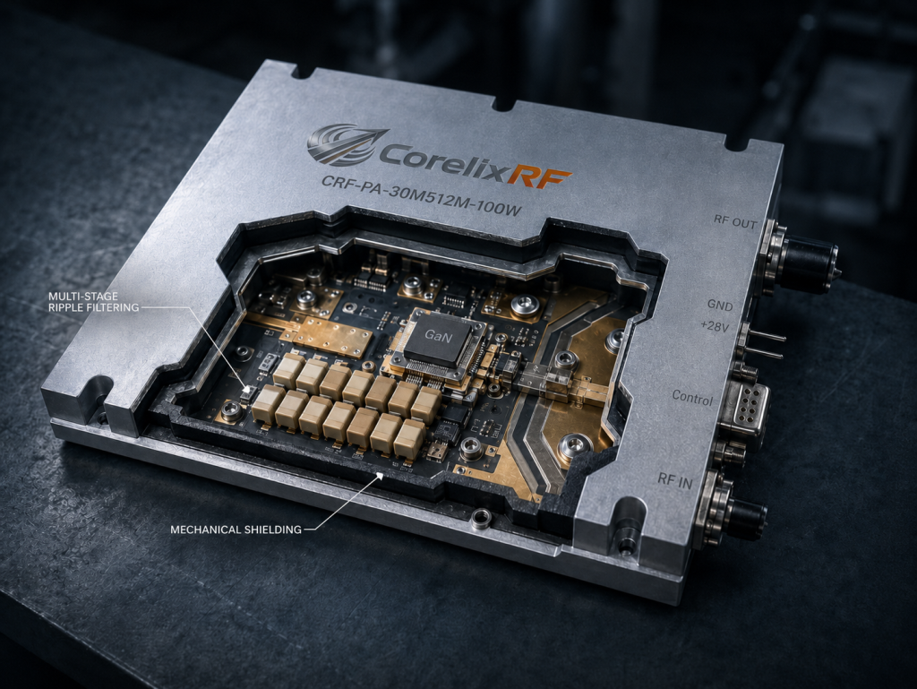
Here is the engineering truth the CRF-PA-30M512M-100W is manufactured specifically to eradicate the vulnerabilities inherent in standard commercial amplification designs by integrating aggressive multi-stage filtering directly into the core printed circuit board architecture. The module utilizes heavy tantalum and ceramic capacitor banks localized precisely at the transistor drain terminals, providing instantaneous charge reservoirs that maintain strict voltage stability during brutal high-duty-cycle radar pulses. This unit guarantees ultra-low distortion across its entire designated broadband spectrum by maintaining a physically impenetrable barrier against low-frequency ripple, ensuring the EVM remains completely pure regardless of the external power supply’s electrical condition. Every internal trace routing and impedance matching network is verified through rigorous full-wave electromagnetic simulation and validated by physical laboratory testing, delivering an unyielding hardware solution for defense and high-precision commercial integrations.
| Model Number | Freq Range | Peak Power Output | EVM Degradation | Operating Voltage |
| CRF-PA-30M512M-100W | 30 – 512 MHz | 100 Watts | < 1.0% | 28V DC |
| Competitor Unit A | 30 – 512 MHz | 85 Watts | > 4.5% | 28V DC |
| Competitor Unit B | 100 – 500 MHz | 90 Watts | > 3.0% | 24V DC |
| CRF-PA-Legacy | 30 – 512 MHz | 50 Watts | < 1.5% | 28V DC |
What Role Does Mechanical Shielding Play In Isolating Supply-Borne Interference?
Mechanical chassis design represents a critical defensive layer that physicalizes the isolation between highly noisy power conversion electronics and sensitive microvolt-level microwave reception and amplification chains. CorelixRF modules are housed in strictly toleranced, heavy-gauge CNC-machined aluminum enclosures featuring integrated microwave absorber materials and EMI-shielding gaskets that prevent radiated electromagnetic fields from coupling into the exposed microstrip lines. Without this rigid mechanical barrier, high-frequency switching transients from power supplies act as transmitting antennas inside the system rack, radiating broadband noise directly into the cavity of the RF amplifier, entirely bypassing the conducted emission filters. Engineering a hermetically sealed or deeply shielded physical environment forces all incoming power to pass strictly through heavy feed-through capacitors, stripping away all high-frequency garbage before it can enter the clean room environment of the final RF amplification stage.
How Do We Verify Radar Operation Within Tolerances Through Strict Laboratory Data?
Verification mandates subjecting every finished amplifier module to a brutal matrix of environmental and electrical stress tests that push the physical hardware far beyond normal expected operational limits. CorelixRF utilizes automated test benches to hammer the amplifiers with severe mismatched loads, verifying that the internal isolators and circulators prevent reflected power from destroying the output transistors during catastrophic antenna failures. Furthermore, continuous thermal cycling in specialized environmental chambers ensures that solder joints, wire bonds, and substrate materials survive the extreme mechanical stresses of thermal expansion and contraction without suffering microscopic fractures. Only after measuring and logging the insertion loss, return loss, and full-power spurious emissions across all temperature extremes do we certify the hardware as ready for deployment in mission-critical radar infrastructure.
| Test Category | Parameter | Physical Stress Applied | Pass/Fail Criteria |
| Thermal Shock | Extremes | -40°C to +85°C cycling | No physical fracturing |
| Mismatch Survival | VSWR | 5:1 load at full power | Zero device failure |
| Spectral Purity | Spurious | Max output, CW mode | < -65 dBc emissions |
| Burn-in | Duration | 72 hours max saturation | Gain stability < 0.2dB |
Conclusion
Mastering the physical deployment of high-power amplification requires abandoning commercial assumptions and facing the harsh realities of thermal dissipation, impedance drift, and catastrophic voltage ripple. Implementing ordinary power architectures directly compromises target tracking resolution, forces rapid component burnout, and destroys the integrity of the baseband signal before it ever reaches the transmitting antenna. CorelixRF engineering provides the rigorous, tested, and physically robust hardware solutions required to survive in these demanding environments, stripping away interference and guaranteeing absolute fidelity under heavy load. Contact the CorelixRF engineering team today to request the official laboratory Data Sheet for the CRF-PA-30M512M-100W and secure your supply chain with manufacturing truth.
FAQ
Q1: Why does GaN technology require stricter power supply filtering than legacy LDMOS amplifiers?
GaN transistors have a significantly higher power density and faster switching speed, making them highly reactive to minute changes in drain and gate voltages. Even low-amplitude ripple will rapidly modulate the output signal, requiring massive localized decoupling capacitance and active bias regulation to maintain stable operation.
Q2: How does CorelixRF measure and validate the EVM purity of the CRF-PA-30M512M-100W?
We connect the output to high-grade vector signal analyzers running complex modulation schemes identical to field deployment parameters. We evaluate the physical constellation spread against known pure baseline signals while simultaneously injecting noise into the power line to verify our internal filtering limits.
Q3: Can digital pre-distortion (DPD) compensate for power supply ripple in a radar system?
No. DPD algorithms are designed to correct deterministic, repeating non-linearities intrinsic to the amplifier’s compression curve. Low-frequency ripple is a continuously varying external artifact that randomly shifts the operating baseline, making it physically impossible for static digital algorithms to mathematically predict and correct.
Q4: What causes the catastrophic failure of commercial power supplies when running pulsed RF loads?
Commercial supplies are designed for static continuous current draw. The instantaneous transition from zero to maximum current during a radar pulse causes massive voltage droop, followed by aggressive overcompensation from the supply’s feedback loop, physically damaging the RF transistors with dangerous voltage spikes.
Q5: How does thermal expansion directly impact the VSWR of the system?
Heat causes the physical substrate materials of the printed circuit boards to expand, altering the strict geometric dimensions of the microstrip transmission lines. This physical change shifts the electrical phase length and characteristic impedance, causing mismatches that reflect energy back into the active devices.
Make the lab setup and report curves part of the RFQ
Test-bench issues become easier to resolve when the RFQ lists signal source, cable loss, load condition, calibration setup, power sequencing, gain flatness, spurious limits and report format.
Recommended next step: send the operating band, output power target, duty cycle, load condition, control interface, protection or thermal limits and required FAT documents. CorelixRF can review this How to Achieve Broadband EVM Purity with Low-Frequency Ripple Suppression? requirement against standard RF amplifier platforms, RF front-end options and controlled customization paths.