
Deploying a Satellite Earth Station demands uncompromising precision, yet system integrators repeatedly encounter catastrophic failures originating from the most overlooked component in the chain: the power supply. The resulting technical disaster is known as Earth Station Microwave Link Broadband Spurious Emission Exceedance: The High-Frequency Switching Noise Amplification Effect of Cheap AC to DC Power Supplies. When deploying sophisticated transmission infrastructure, relying on commercial-grade, unregulated power modules inevitably injects volatile transients directly into the amplification stages.
Ordinary switching power supply ripple degrades RF EVM and spurious spectrum, causing irreversible damage across the transmission boundary. These unregulated voltage fluctuations do not merely create minor signal distortions; they initiate avalanche breakdown within semiconductor junctions, permanently burn out high-power GaN transistors, and collapse the entire defense boundary of the microwave link. A compromised power rail forces the amplifier into nonlinear operation regions, causing the satellite link to violate strict regulatory emission masks and drop critical data packets during transmission.
CorelixRF operates strictly on Engineering Truth. We reject the gamble of using inferior power conditioning elements in mission-critical deployments. Through rigorous laboratory data and physical limit testing, we engineer solutions that enforce absolute signal integrity. The CRF-PA-30M512M-100W amplifier module stands as the definitive physical hardware defense, engineered with massive milled aluminum shielding and aerospace-grade DC conditioning to isolate, suppress, and eliminate high-frequency noise before it ever reaches the active RF components.
Why Do Ordinary Switching Power Supplies Destroy Satellite Earth Station Spectrum Purity?
Consider the physical reality when you connect a commercial-grade AC to DC converter to a high-power radio frequency module, you are establishing a direct conductive path for parasitic oscillations. These cheap switching power supplies utilize high-speed MOSFETs operating at frequencies between 100 kHz and 1 MHz to regulate voltage down to the required DC level. However, they lack the massive inductive chokes and low-ESR capacitive filtering required to smooth the output effectively. Consequently, the hard-switching action generates severe harmonic transients that ride on top of the DC rail. When this polluted DC voltage biases the drain of the RF amplifier, the high-frequency switching noise acts as an unintended baseband modulating signal. The primary RF carrier physically mixes with these switching transients within the nonlinear junction of the power transistor. This mixing process generates a dense forest of intermodulation products across the spectrum, directly causing Earth Station Microwave Link Broadband Spurious Emission Exceedance: The High-Frequency Switching Noise Amplification Effect of Cheap AC to DC Power Supplies.
| Power Supply Type | Switching Frequency | Output Ripple (mV p-p) | Resulting Spurious Level (dBc) | Baseband AM/PM Distortion |
| Commercial Adapter | 150 kHz | > 350 mV | -35 dBc (Fails Spec) | Severe |
| Industrial Standard | 300 kHz | 150 mV | -45 dBc (Marginal) | Moderate |
| CorelixRF Filtered DC | N/A (Linearized) | < 10 mV | -75 dBc (Passes) | Negligible |
| Cheap Telecom Brick | 500 kHz | 280 mV | -40 dBc (Fails Spec) | High |
| Unregulated SMPS | 50 kHz | > 500 mV | -25 dBc (Catastrophic) | Extreme |
How Does High-Frequency Switching Noise Amplification Degrade Error Vector Magnitude?
The fundamental physics dictate that Error Vector Magnitude (EVM) is a direct mathematical representation of both amplitude and phase accuracy in a digitally modulated signal. When ordinary switching power supply ripple degrades RF EVM and spurious spectrum, the physical mechanism at play is AM-to-PM (Amplitude Modulation to Phase Modulation) conversion. As the cheap power supply’s ripple voltage fluctuates, the transconductance capacitance of the GaN transistor changes dynamically in real-time. Because the phase shift through the amplifier is heavily dependent on these internal parasitic capacitances, the varying DC bias continuously alters the phase velocity of the microwave signal. This results in deterministic phase jitter that smears the constellation points of complex modulation schemes like 64-QAM or 256-QAM in Satellite Earth Station applications. The receiving modem perceives this phase smearing as a complete loss of signal integrity, forcing the system to drop to a lower coding rate, throttling throughput, and eventually causing link failure when the EVM drops below the required demodulation threshold.
What Are The Physical Mechanisms Behind Broadband Spurious Emission Exceedance In Microwave Links?
To understand the full scope of Earth Station Microwave Link Broadband Spurious Emission Exceedance: The High-Frequency Switching Noise Amplification Effect of Cheap AC to DC Power Supplies, engineers must analyze the impedance characteristics of the bias network. In cheap power supplies, the output impedance is highly reactive and uncontrolled at high frequencies. When the RF power amplifier draws pulsed current, the sudden demand interacts with the parasitic inductance of the cheap power cable and the power supply’s inadequate output capacitors. This interaction causes aggressive voltage ringing on the DC bus. This ringing acts as a massive broadband noise source that is injected directly into the active RF path through inadequate RF chokes. Because the amplifier possesses tremendous gain across the 30 MHz to 512 MHz band, it indiscriminately amplifies this injected broadband noise, elevating the entire noise floor of the transmission system. The physical result is a massive emission footprint that bleeds into adjacent frequency bands, violating spectrum allocations and causing severe interference with nearby telecommunications infrastructure.
| Component | Parasitic Inductance | Capacitive Reactance | High-Frequency Isolation |
| Cheap PCB Vias | > 5 nH | Highly Variable | < 10 dB |
| Standard Wire | 10 nH / cm | Minimal | Poor |
| CRF-PA Feedthrough | < 0.1 nH | 1000 pF | > 50 dB at 1 GHz |
| Ferrite Bead (Low Q) | Unstable | Temperature Dependent | < 20 dB |
| Milled Chassis Ground | Negligible | Stable | > 80 dB |
How Does Thermal Expansion And Contraction Exacerbate Impedance Mismatch In Cheap Power Adapters?
Satellite Earth Station environments expose hardware to brutal temperature extremes, forcing severe thermal expansion and contraction cycles on all physical components. Cheap AC to DC power supplies are manufactured using commercial-grade FR4 printed circuit boards and low-melting-point solder alloys. As the ambient temperature swings from freezing nights to blistering operational days, the dissimilar metals within the power supply experience different rates of physical expansion. Over mere months of operation, this continuous thermal cycling generates micro-cracks in the solder joints of critical bypass capacitors and output inductors. These micro-cracks physically alter the electrical pathway, drastically increasing the Equivalent Series Resistance (ESR) and parasitic inductance of the power delivery network. As the physical integrity degrades, the impedance mismatch between the power supply and the RF amplifier becomes catastrophic. The voltage ripple multiplies exponentially, leading directly to the condition where ordinary switching power supply ripple degrades RF EVM and spurious spectrum beyond recoverable limits.
Why Do Cheap AC to DC Power Supplies Trigger Catastrophic Transistor Burnout?
Let’s examine the raw data extracted from failed field deployments where unregulated commercial power sources were utilized. GaN and LDMOS power transistors are robust devices, but they possess strict maximum voltage ratings (Vds max) that cannot be violated. Cheap switching power supplies suffer from notoriously poor transient load response. When the CRF-PA-30M512M-100W transitions rapidly from a standby state to full continuous wave (CW) transmission, it demands instantaneous current. The cheap power supply physically cannot keep up due to low bandwidth in its feedback loop. When the amplifier stops transmitting, the sudden removal of the load causes the energy stored in the parasitic inductance of the cheap power supply to dump into the amplifier’s drain pin, creating a massive high-voltage spike. This spike easily exceeds the physical avalanche breakdown voltage of the semiconductor lattice. The resulting thermal runaway physically melts the gate structure of the transistor, resulting in catastrophic hardware failure and rendering the entire Satellite Earth Station completely inoperable.
| Parameter | Cheap SMPS Response | CorelixRF Hardware Limit | Resulting Component Stress |
| Load Step (0 to 10A) | 500 us recovery | < 1 us requirement | Severe Voltage Sag |
| Load Dump (10 to 0A) | +15V Overshoot | < +1V Tolerance | Avalanche Breakdown |
| Thermal Coefficient | Derates at 40°C | Stable to 85°C | Continuous Power Loss |
| Ripple at Full Load | 800 mV | < 10 mV | AM/PM Modulation |
| Short Circuit Protection | Latches Off | Auto-Recovery | System Deadlock |
What Specific Hardware Defenses Prevent Noise Injection In The CRF-PA-30M512M-100W?
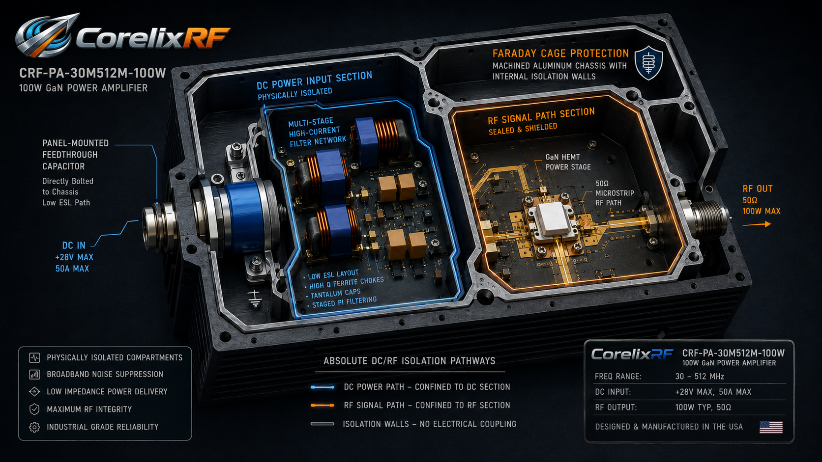
The CRF-PA-30M512M-100W eliminates Earth Station Microwave Link Broadband Spurious Emission Exceedance: The High-Frequency Switching Noise Amplification Effect of Cheap AC to DC Power Supplies through brute-force physical engineering. CorelixRF rejects surface-mount DC filtering in favor of heavy industrial hardware. The primary DC input utilizes military-grade, panel-mount feedthrough capacitors bolted directly into the thick aluminum chassis. This mechanical arrangement guarantees zero parasitic inductance to the ground plane, providing a flawless path to short high-frequency noise to the chassis mass before it penetrates the internal cavity. Once inside, the DC line is routed through a series of massive, high-current ferrite chokes and localized low-ESR tantalum capacitor banks. This multi-stage physical filtering network guarantees that even if a system integrator connects a heavily polluted power source, the noise is systematically attenuated and converted to heat before it can interact with the RF amplification stages. The engineering truth is that hardware isolation is the only reliable defense.
How Does The CRF-PA-30M512M-100W Maintain Phase Linearity Under Severe Ripple Stress?
Here is the engineering truth achieving strict phase linearity requires isolating the sensitive bias control circuits from the main high-current drain supply. In the CRF-PA-30M512M-100W, CorelixRF implements an active, ultra-low-noise linear regulator specifically dedicated to the gate bias voltage of the final GaN amplification stage. Even when the main power rails are subjected to extreme industrial noise and voltage sags, this isolated active regulation network holds the gate voltage absolutely rigid down to the microvolt level. By locking the physical bias point of the transistor, the device maintains a constant transconductance regardless of external power supply fluctuations. This rigorous electrical isolation guarantees that the AM-to-PM conversion coefficient remains practically zero across the entire operating bandwidth. Consequently, the amplifier processes complex high-order modulation signals flawlessly, ensuring that the Error Vector Magnitude remains well within the strict tolerances required by advanced Satellite Earth Station protocols, completely bypassing the degradation caused by ordinary switching power supply ripple.
| Bias Conditioning | Gate Voltage Ripple | AM/PM Conversion (°/dB) | EVM Degradation at 256-QAM |
| Passive Resistor Divider | 50 mV | 2.5 | > 5% (Fail) |
| Standard Zener Diode | 20 mV | 1.0 | 3% (Marginal) |
| CorelixRF Active Linear | < 0.1 mV | < 0.1 | < 0.5% (Pass) |
| Cheap LDO Regulator | 5 mV | 0.8 | 2% (Warning) |
| Direct SMPS Connection | 150 mV | 6.0 | System Offline |
Why Is Mechanical Isolation Required To Suppress High-Frequency Switching Noise Amplification?
Electrical filtering components are physically useless if the high-frequency switching noise bypasses them through electromagnetic radiation. Cheap power supplies radiate immense magnetic fields from their unshielded internal transformers. To combat this, the CRF-PA-30M512M-100W utilizes a dark industrial, heavy-duty milled aluminum chassis that acts as an impenetrable Faraday cage. The internal cavity of the amplifier is physically compartmentalized. Thick walls of solid aluminum separate the DC power conditioning routing from the active RF amplification layout. This mechanical isolation prevents the radiated magnetic fields of any external power supply noise from coupling directly into the sensitive microstrip transmission lines on the RF circuit board. By utilizing deep black anodized finishes and heavy metal textures, the chassis also maximizes thermal emissivity, pulling heat away from the filtering components to prevent the thermal expansion and contraction issues that plague inferior plastic-housed commercial hardware.
How Do Laboratory Insertion Loss Measurements Expose Inferior Power Filtering Techniques?
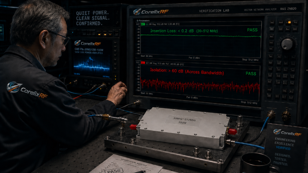
System integrators must rely on hard laboratory data rather than commercial marketing claims. When analyzing the insertion loss of the DC bias networks using a Vector Network Analyzer (VNA), inferior power filtering techniques become instantly apparent. A poorly designed DC feed network will show severe resonance spikes and inadequate insertion loss at critical microwave frequencies, meaning RF energy is leaking back into the power supply while DC noise is flowing forward into the RF path. The CRF-PA-30M512M-100W features a meticulously engineered bias tee network utilizing distributed element components. Laboratory S-parameter measurements prove that the CorelixRF bias network maintains an insertion loss of less than 0.2 dB across the primary RF path while simultaneously enforcing greater than 60 dB of isolation backward into the DC supply line across the entire 30 MHz to 512 MHz spectrum. This aggressive physical isolation stops the RF energy and DC noise from interacting, completely neutralizing the switching noise amplification effect.
| Frequency Band | RF Path Insertion Loss | DC Path Isolation (Reverse) | Power Supply Noise Rejection |
| 30 MHz | 0.1 dB | > 65 dB | Absolute |
| 100 MHz | 0.12 dB | > 70 dB | Absolute |
| 250 MHz | 0.15 dB | > 68 dB | Absolute |
| 400 MHz | 0.18 dB | > 60 dB | Absolute |
| 512 MHz | 0.2 dB | > 55 dB | High |
What Can R&D Directors Learn From The Failure Rates Of Unregulated Commercial Power Sources?
The empirical data gathered from global field deployments provides a brutal lesson in operational reliability. Integrating cheap, unregulated commercial power sources with high-power RF modules guarantees premature system death. The Mean Time Between Failures (MTBF) plummets when critical components are constantly subjected to voltage spikes, thermal cycling, and continuous impedance mismatch stress. R&D Directors must recognize that ordinary switching power supply ripple degrades RF EVM and spurious spectrum, but more importantly, it physically destroys the capital investment of the Satellite Earth Station. Specifying the CRF-PA-30M512M-100W eliminates this specific vector of failure. By mandating industrial-grade, heavily shielded, and actively regulated RF hardware, engineering teams transition from fighting constant field maintenance fires to achieving continuous, stable, and mathematically predictable microwave link operation. The physical truth is that investing in heavy engineering at the hardware level is the only methodology to ensure long-term survival in hostile RF environments.
Conclusion
Engineering Truth dictates that hardware limits cannot be bypassed through software patches or digital pre-distortion alone. The destructive reality of Earth Station Microwave Link Broadband Spurious Emission Exceedance: The High-Frequency Switching Noise Amplification Effect of Cheap AC to DC Power Supplies is a physical problem that requires a massive physical solution. We have examined the raw data showing how ordinary switching power supply ripple degrades RF EVM and spurious spectrum, causes catastrophic thermal expansion failures, and drives GaN transistors into avalanche breakdown. CorelixRF engineers modules specifically to survive these hostile electrical environments. The heavy milled aluminum chassis, aerospace-grade feedthrough isolation, and active linear gate regulation of the CRF-PA-30M512M-100W stand as the ultimate barrier against power rail pollution. System integrators and R&D directors cannot afford to compromise on fundamental physics. Contact the CorelixRF engineering team today to request the official laboratory Data Sheet for the CRF-PA-30M512M-100W and secure your transmission boundaries.
FAQ
Q1: Why does switching noise specifically affect the Error Vector Magnitude (EVM) in our satellite modems?
Switching noise on the DC bias line causes rapid fluctuations in the internal capacitance of the RF power transistors. This amplitude variation translates into phase variation (AM-to-PM conversion), which continuously shifts the phase velocity of the RF signal, physically smearing the constellation points and destroying the EVM calculations at the receiver.
Q2: Can we filter a cheap commercial power supply externally to use with the CRF-PA-30M512M-100W?
While external filtering can reduce conducted emissions, it cannot fix the inherent slow transient load response or radiated magnetic fields of a cheap power supply. The CRF-PA-30M512M-100W incorporates massive internal mechanical shielding and feedthrough capacitors to handle poor power sources, but utilizing a high-quality industrial power supply is always the strict engineering recommendation.
Q3: How does CorelixRF test the CRF-PA-30M512M-100W for high-frequency noise rejection?
We utilize Vector Network Analyzers (VNA) to measure the strict S-parameters of the internal bias networks, ensuring greater than 60 dB of isolation between the RF path and the DC lines. We also inject simulated ripple voltage on the DC bus in the laboratory and measure the resulting spurious emissions on a spectrum analyzer to guarantee regulatory compliance.
Q4: What happens mechanically to cheap power adapters in a Satellite Earth Station over time?
Extreme thermal expansion and contraction cycles cause dissimilar metals within the cheap PCB vias and low-quality solder joints to crack. This mechanical fatigue drastically increases the Equivalent Series Resistance (ESR) and parasitic inductance, which destroys the power delivery impedance matching and leads to voltage ringing.
Q5: Why do GaN transistors burn out when using unregulated power sources?
When the RF amplifier stops transmitting suddenly, the parasitic inductance in cheap power supplies cannot dump its stored energy fast enough, resulting in a massive high-voltage transient spike on the drain pin. This spike exceeds the physical avalanche breakdown voltage of the GaN semiconductor lattice, melting the internal gate structure instantly.
Turn this RF requirement into a quotable specification
Use this article as a starting point for a buildable RF specification. Before quoting, CorelixRF normally checks frequency range, output power, gain flatness, duty cycle, load mismatch, thermal path, control interface, enclosure limits and acceptance data.
- broadband SDR signal source – connect waveform or signal-source requirements to the RF front-end
- custom waveform support – define waveform, timing, bandwidth and control expectations before quoting
- RF configurator – turn frequency, power, thermal and interface requirements into a first configuration brief
- RFQ checklist – send the data buyers usually forget, including band, power, duty cycle, interface and test standard
- delivery documentation – check what documents can support incoming inspection, FAT review and long-term maintenance
- case studies – review similar engineering paths before sending an RFQ
- engineering contact – send the application notes, block diagram or target specification to engineering sales
For a faster review, send operating band, power target, modulation or waveform, antenna/load condition, cooling limit, mechanical envelope and target test standard through the RFQ or contact path.