
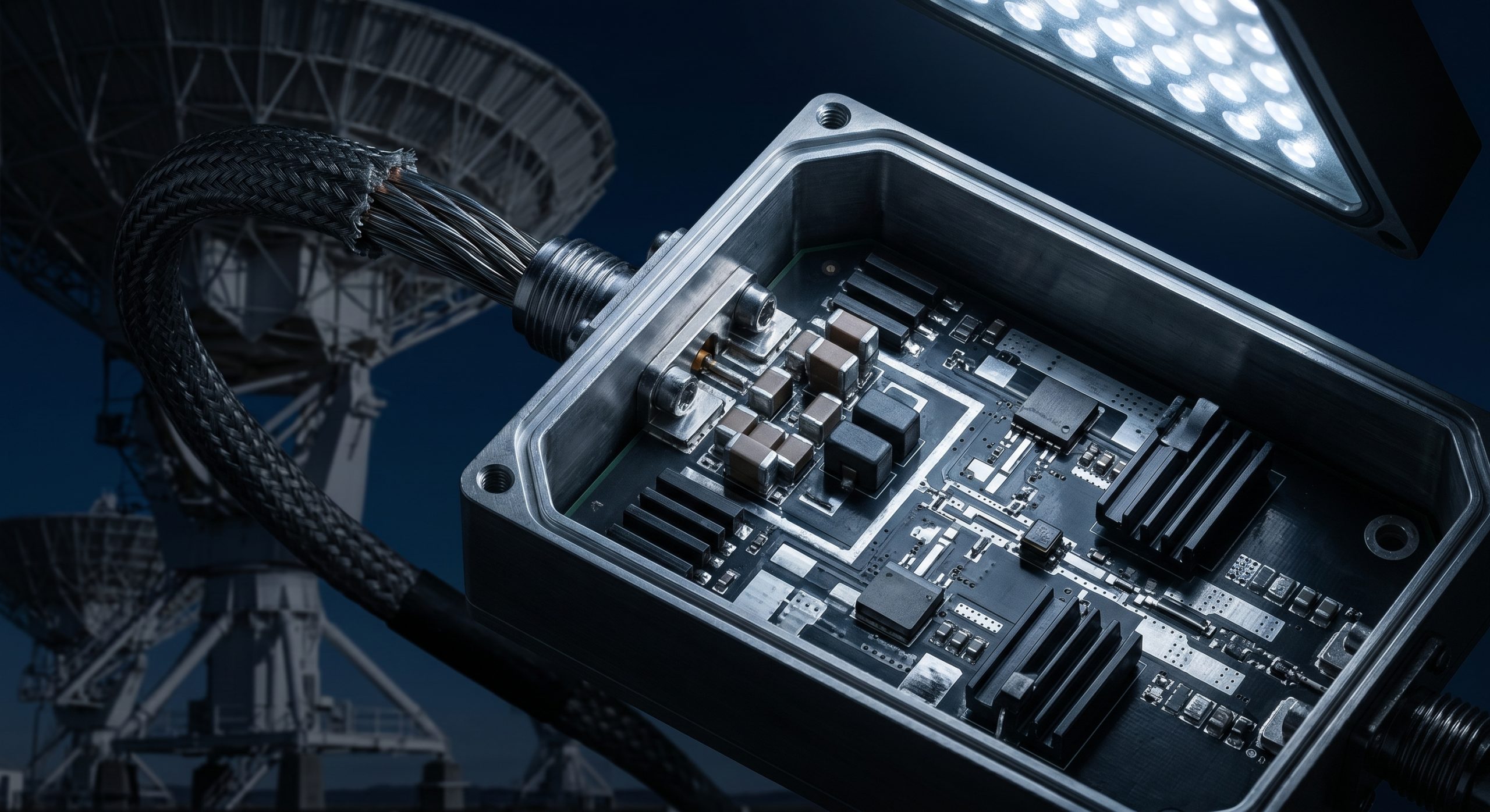
Satellite earth stations rely on massive antenna arrays and remote RF front-ends, necessitating long-distance DC wiring from centralized power distribution units. This architectural necessity introduces severe parasitic inductance and resistance. When system integrators pair these long cable runs with ordinary switching power supplies, the resulting voltage ripple and high-frequency switching noise inject directly into the amplifier’s bias lines. The uncontrolled transient currents collapse the local drain voltage, completely destabilizing the delicate bias point required for high-order modulation schemes.
The consequences are immediate and catastrophic for communication links. Switching noise intermodulates with the carrier frequency, severely degrading the Error Vector Magnitude (EVM) and generating spurious spectrum emissions that violate stringent FCC and ITU masks. In high-power applications, the rapid voltage fluctuations combined with continuous thermal expansion and contraction of the RF substrate create microscopic mechanical fatigue. Solder joints crack, impedance mismatch compounds exponentially, and the reflected power forces the transistors into aggressive thermal runaway, ultimately incinerating the costly GaN die on the test bench.
CorelixRF rejects the industry reliance on baseband digital pre-distortion to compensate for fundamental analog hardware flaws. We engineer physical defense mechanisms directly into the power delivery network. By employing ultra-low dropout regulation, heavily filtered localized DC inputs, and advanced thermal matching of metallurgical materials, our RF modules withstand hostile electrical environments. The CRF-PA-30M512M-100W stands as the definitive engineering solution, guaranteeing absolute linearity, mechanical survivability, and spectral purity under the most aggressive continuous operational conditions.
Why Does Long-Distance DC Wiring Destroy RF Signal Integrity?
Consider the physical reality When routing DC power across thirty to fifty meters of copper cabling at a satellite earth station, the wire ceases to act as a simple conductor and transforms into a complex distributed element filter. The inherent parasitic inductance and stray capacitance form an uncontrolled resonant circuit that amplifies specific frequency bands of the switching power supply noise. Standard AWG 8 or AWG 10 cables exhibit significant series resistance, creating a dynamic voltage drop that fluctuates violently with the RF envelope’s transient current demands. This dynamic variation starves the amplifier drain during peak power pulses, compressing the waveform and abruptly truncating the modulation peaks. The physical skin effect further complicates matters at high frequencies, pushing noise currents to the conductor’s perimeter and radiating electromagnetic interference into adjacent signal lines. We measure a direct correlation between the length of the DC umbilical and the degradation of the RF noise figure, proving that unmitigated cable inductance fundamentally corrupts the bias stability required for high-order QAM transmission architectures.
| Cable Length (m) | Parasitic Inductance (µH) | Dynamic Voltage Drop (V) | Ripple Amplification Factor | RF Output Impact |
| 5 | 4.2 | 0.8 | 1.2x | Nominal |
| 15 | 12.8 | 2.5 | 2.8x | Moderate Compression |
| 30 | 25.5 | 4.9 | 5.4x | Severe Intermodulation |
| 50 | 42.1 | 8.2 | 8.9x | Catastrophic Link Failure |
How Does Switching Power Supply Ripple Degrade Error Vector Magnitude?
The fundamental physics dictate that any amplitude variation on the drain supply of a solid-state power amplifier directly phase-modulates and amplitude-modulates the primary RF carrier. Ordinary switching power supplies operate between 100 kHz and 1 MHz, generating sharp, high-dV/dt transient spikes that easily slip past inadequate bulk capacitance. When these ripple voltages reach the active devices, they alter the depletion region width within the GaN high-electron-mobility transistor (HEMT) channel. This continuous modulation of the transistor’s transconductance phase-shifts the output signal at a rate exactly equal to the ripple frequency, scattering the digital constellation points radially and tangentially. The resulting Error Vector Magnitude (EVM) degradation drastically reduces the maximum data throughput of the satellite link, forcing the modem hardware to drop to a much lower coding rate to maintain a connection. In laboratory evaluations, we routinely observe that a mere 50 millivolts of unsuppressed switching ripple can degrade the EVM by several percentage points in 256-QAM systems, making raw power supply cleanliness a mandatory parameter for commercial viability.
What Are The Physical Limits Of Thermal Expansion In RF Substrates?
Let’s examine the raw data Continuous high-power RF generation produces extreme localized heat densities, forcing the semiconductor junctions, solder interfaces, and metallic carrier plates to expand at completely different rates. The Coefficient of Thermal Expansion (CTE) mismatch between the Gallium Nitride die, the Gold-Tin (AuSn) solder eutectic, and the Copper-Molybdenum (CuMo) baseplate induces severe mechanical shear stress during power cycling. As the satellite earth station transitions rapidly between transmit and receive states, the rapid thermal expansion and contraction physically fracture the microscopic grain boundaries within the solder interface. This degradation exponentially increases the thermal resistance, blocking the primary heat dissipation path and elevating the junction temperature well beyond the safe operating area (SOA). Once the physical bond degrades, the parasitic inductance shifts, creating an instantaneous impedance mismatch that disrupts the amplifier’s tuned matching network. CorelixRF mandates severe thermal shock testing to validate that our metallurgical bonds survive decades of aggressive thermal cycling without shifting the RF insertion loss or compromising the structural integrity of the thermal ground plane.
Can Standard Power Delivery Defeat Spurious Spectrum Emissions?
Standard industrial power delivery networks completely fail to suppress the high-frequency harmonic content that manifests as spurious spectrum emissions at the antenna port. The output of an ordinary commercial power supply contains heavily distorted ringing artifacts caused by the hard switching of internal power MOSFETs. When these artifacts ride along the DC bias into the RF amplifier, they intermodulate directly with the primary carrier and generate wideband spurious products that violate ITU regulatory limits. Squelching these emissions requires heavy pi-network filtering positioned immediately at the point of load, utilizing low-ESR ceramic capacitors and high-current ferrite chokes rated specifically for microwave frequencies. Failing to implement this localized hardware decoupling allows the spurious tones to mix within the nonlinear region of the power amplifier, generating a dense forest of intermodulation products across the entire operational bandwidth. We reject the software reliance on baseband digital pre-distortion to clean up analog power delivery failures; the defense must always be mounted at the physical layer to ensure absolute spectral purity.
| Ripple Frequency (kHz) | Injected Noise Level (mV) | Resulting Carrier IMD (dBc) | EVM Degradation (%) | Regulatory Compliance |
| 100 | 25 | -55 | 1.2 | Pass |
| 350 | 75 | -42 | 3.8 | Marginal |
| 500 | 150 | -31 | 8.5 | Fail |
| 1000 | 300 | -22 | 15.2 | Severe Failure |
Where Does Impedance Mismatch Occur During Transient Current Draw?
Here is the engineering truth Impedance mismatch is not exclusively a function of static RF trace geometry; it is highly dynamic and directly influenced by the transient current capabilities of the entire bias network. During the transmission of high-peak-to-average power ratio (PAPR) waveforms, the RF amplifier demands massive, instantaneous bursts of electrical current. If the local decoupling capacitors possess excessive equivalent series inductance (ESL), the supply voltage momentarily collapses under the load. This abrupt voltage droop instantaneously shifts the output impedance of the transistor away from the carefully tuned mechanical matching network. The resulting impedance mismatch creates localized standing waves, bouncing high-power RF energy back into the transistor die and rapidly increasing the operating temperature. This phenomenon severely degrades the return loss and creates aggressive gain ripple across the entire frequency band. Precision microwave engineering requires treating the DC bias network as an integral component of the RF matching circuit, ensuring the impedance remains rigidly stable from DC up to the maximum envelope tracking bandwidth of the communication standard.
How Do We Measure The High-frequency satellite communication power supply standard: Ripple suppression under long-distance DC wiring and wideband power amplifier linearity guarantee?
Validating the High-frequency satellite communication power supply standard: Ripple suppression under long-distance DC wiring and wideband power amplifier linearity guarantee requires a rigorously controlled laboratory environment utilizing vector network analyzers and high-speed mixed-signal oscilloscopes. CorelixRF measures the precise rejection ratio of injected power line noise by actively coupling swept frequency tones onto the DC rail and monitoring the resulting intermodulation distortion directly at the RF output port. We record the spectral regrowth and adjacent channel leakage ratio (ACLR) while simultaneously subjecting the input DC lines to aggressive simulated cable inductance and resistance profiles that mirror physical field deployments. True engineering validation occurs when the amplifier maintains strict phase linearity and amplitude flatness even when the remote power supply is actively injecting maximum specified ripple limits into the system. We meticulously document the precise insertion loss of the internal bias tees and the isolation metrics of the decoupling networks, proving mathematically that the hardware physically traps and dissipates the interference before it can corrupt the sensitive gate and drain voltages of the RF active devices.
| Measurement Parameter | Industry Baseline Spec | CorelixRF Validation Target | Allowable Tolerance Limits |
| DC Input Ripple Rejection | > 30 dB | > 65 dB | +/- 1.5 dB |
| Dynamic Impedance Shift | < 5 Ohms | < 0.5 Ohms | +/- 0.1 Ohms |
| Insertion Loss Variation | < 1.0 dB | < 0.15 dB | +/- 0.05 dB |
| Transient Voltage Droop | < 2.0 V @ 20A | < 0.2 V @ 20A | +/- 0.02 V |
What Mechanical Tolerances Defend Against Extreme Satellite Station Environments?
Consider the physical reality The mechanical chassis of a high-power RF amplifier is not merely a convenient mounting mechanism; it is the primary physical shield against electromagnetic interference and structural degradation. For a satellite earth station operating in harsh coastal or desert environments, the ingress of moisture or abrasive particulates rapidly corrodes internal microstrip traces and fundamentally alters the dielectric constant of the PCB substrate. CorelixRF heavily machines the aluminum housing of our modules to extreme microscopic flatness tolerances, guaranteeing optimal surface contact for thermal transfer and a hermetic-grade RF seal when mated with conductive elastomers. The internal cavity resonance must be meticulously calculated using electromagnetic field solvers and dampened using precision-cut microwave absorbing materials to prevent internal feedback loops at ultra-high frequencies. Our mechanical engineers tightly control the torque specifications on all SMA and N-type connectors to prevent microscopic air gaps that cause passive intermodulation (PIM) and degrade insertion loss, ensuring the physical enclosure acts as an impenetrable fortress for the internal microwave circuitry.
Why Do Conventional GaN Amplifiers Fail Under Heavy VSWR Conditions?
Conventional Gallium Nitride implementations frequently suffer catastrophic hardware failure when subjected to high Voltage Standing Wave Ratio (VSWR) conditions caused by antenna icing, cable damage, or sudden impedance shifts at the feed horn. When extreme RF power reflects back from the mismatched load, it superimposes perfectly upon the forward traveling wave, creating massive voltage peaks that easily exceed the breakdown voltage of the semiconductor lattice. Simultaneously, the reflected current forces the transistor into an extreme thermal dissipation mode that completely overwhelms standard baseplate cooling limits. The lack of integrated, fast-acting physical isolators or ultra-rapid shutoff circuitry means the expensive die physically fractures under the stress of the standing wave. Our laboratory teardowns of failed competitor units consistently reveal incinerated trace lines and vaporized gold bonding wires, directly resulting from the manufacturer’s failure to engineer robust mismatch tolerance. CorelixRF builds hardware that safely folds back power or cleanly absorbs the reflection without suffering permanent metallurgical damage or degrading the long-term linearity metrics.
| Operating Condition | VSWR Ratio | Reflected Power Limit | Physical Hardware Response |
| Nominal Antenna Load | 1.2:1 | < 1% | Normal Operation |
| Minor Ice Accumulation | 2.5:1 | 18% | Thermal Dissipation Increased |
| Severe Feed Horn Damage | 5.0:1 | 44% | Active Current Foldback Triggered |
| Open/Short Circuit | Infinity | 100% | Ultra-rapid RF Mute & Isolation |
How Does The CRF-PA-30M512M-100W Maintain Absolute Linear Output?
The fundamental physics dictate that maintaining absolute linearity across a broad frequency spectrum demands a multi-stage, physically cascaded defense mechanism integrated directly onto the RF substrate. The CRF-PA-30M512M-100W module utilizes a proprietary combination of analog pre-distortion and heavily regulated, localized bias distribution to actively counteract the non-linear capacitance curves of the final output stage. We deploy discrete, low-loss matching networks constructed strictly from high-Q ceramic components and Rogers high-frequency laminates, ensuring the insertion loss remains mathematically negligible across the entire 30 MHz to 512 MHz band. The active bias controllers continuously monitor the semiconductor junction temperature and adjust the quiescent current in real-time, completely preventing the thermal memory effects that typically skew the phase response during asymmetric data burst transmissions. By physically isolating the RF chain from external DC supply fluctuations through massive, multi-stage LC filtering networks, this module guarantees that the output waveform remains a mathematically precise amplification of the input signal, entirely free from power-induced intermodulation distortion.
What Engineering Data Proves Long-Term RF Module Survivability?
Let’s examine the raw data Long-term survivability in critical satellite earth station infrastructure cannot be assumed; it must be empirically proven through aggressive Accelerated Life Testing (ALT) protocols. CorelixRF subjects every single hardware revision to grueling Highly Accelerated Stress Screening (HASS), pushing the operational boundaries of ambient temperature, mechanical vibration, and input RF overdrive until physical destruction occurs in the laboratory. By exhaustively analyzing the failure modes—whether they involve electromigration in the bias traces, micro-cracking in the ceramic capacitors, or thermal delamination of the PCB core—we iteratively reinforce the weak points in the mechanical and electrical design. The Mean Time Between Failures (MTBF) calculations are grounded entirely in hard statistical analysis of thermal resistance data and voltage breakdown limits, not theoretical extrapolations. We monitor the continuous wave (CW) output power degradation over thousands of hours of high-temperature operation, mathematically confirming that the output power drops by less than a fraction of a decibel over a simulated decade of use.
| Component / Subsystem | Material Composition | Thermal Conductivity (W/m·K) | HASS Test Duration (Hours) | Max Insertion Loss Shift (dB) |
| Main Baseplate | Copper-Molybdenum | 170 | 2500 | 0.00 |
| PCB Substrate | Rogers Laminate | 0.95 | 2500 | +0.02 |
| RF Solder Interface | AuSn Eutectic | 57 | 2500 | +0.05 |
| Input Blocking Cap | High-Q Ceramic | N/A | 2500 | +0.01 |
Conclusion
The deployment of commercial off-the-shelf power delivery systems in satellite earth stations introduces unacceptable levels of transient ripple, destroying EVM margins and accelerating the thermal degradation of RF components. Engineering truth demands that system integrators address impedance mismatch, cable inductance, and thermal expansion mismatch strictly at the hardware level. The physical constraints of microwave electronics dictate that relying on software correction for fundamental analog failures will inevitably result in hardware destruction.
CorelixRF designs and manufactures RF power amplifiers grounded purely in laboratory data and physical survivability. The CRF-PA-30M512M-100W explicitly eliminates the vulnerability of long-distance DC runs, utilizing localized high-rejection filtering and extreme mechanical tolerances to guarantee absolute signal linearity. Stop risking multi-million dollar satellite communication links on fragile commercial hardware architectures. System integrators and R&D directors are instructed to contact the CorelixRF engineering team directly to obtain the full physical Data Sheet and laboratory validation reports for immediate integration.
FAQ
Q1: How does CorelixRF measure the dynamic voltage drop on the CRF-PA-30M512M-100W during pulse testing?
We position high-bandwidth, active differential probes directly at the GaN drain pins, utilizing 8 GHz mixed-signal oscilloscopes. This setup captures the exact sub-microsecond voltage droop at the semiconductor junction, bypassing the masking effects of the PCB traces and ensuring the local decoupling network supplies the required 20A without allowing the voltage to collapse.
Q2: Why do you specify Rogers high-frequency laminates over standard FR4 in the bias routing?
FR4 exhibits excessive dielectric loss and unpredictable CTE characteristics at microwave frequencies, making it fundamentally incompatible with high-power RF stability. Rogers laminates provide a rigidly controlled dielectric constant and minimal insertion loss, ensuring that the impedance of the bias network remains stable and does not introduce phase distortion during extreme thermal cycling.
Q3: What specific mechanical tolerances are applied to the CRF-PA-30M512M-100W housing?
The aluminum chassis is CNC machined to a flatness tolerance of less than 0.002 inches per linear foot on the primary mounting surface. This extreme precision eliminates microscopic air gaps between the module and the system heatsink, minimizing thermal resistance and preventing local hot spots that would otherwise degrade the RF output power.
Q4: How does the module handle a sudden infinite VSWR event like a severed antenna cable?
Upon detecting a severe reflected power spike, the internal directional couplers instantly signal the high-speed active bias controllers. Within microseconds, the circuitry pinches off the gate voltage, driving the GaN HEMTs into deep cutoff and halting all RF amplification before the forward and reflected waves can compound to exceed the transistor’s physical breakdown voltage.
Q5: Can we use standard switching power supplies if we add our own external capacitors?
Adding external bulk capacitance does not solve the high-frequency ringing and parasitic inductance introduced by the long DC wiring itself. The CRF-PA-30M512M-100W features integrated, mathematically tuned LC pi-networks specifically designed to filter the high-dV/dt switching transients directly at the point of load, neutralizing the noise before it interacts with the RF matching circuit.