
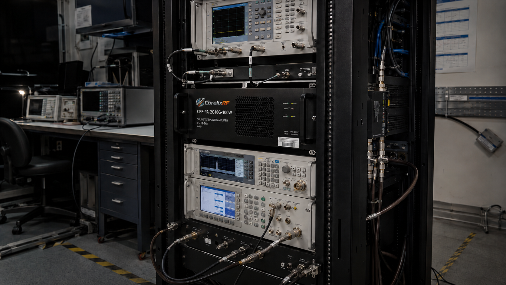
Entering an anechoic chamber for Antenna OTA characterization often brings unexpected signal collapse during X-band sweeps. System integrators regularly observe vector network analyzer curves dropping unpredictably when utilizing non-standard external pads. This gain flatness distortion fundamentally stems from cascading uncalibrated attenuators within complex RF front-end architectures. Our analysis directly targets these impedance mismatch anomalies disrupting your critical radar payload calibrations. CorelixRF presents an engineered hardware matching logic relying on rigorous component selection protocols. Utilizing precision power amplifier modules eliminates downstream instrumentation measurement errors entirely. I have spent two decades troubleshooting these exact microwave laboratory failures. We build solid transmission networks grounded strictly in verifiable engineering truth. Here’s a deal: standard commercial components simply fail under demanding pulsed waveform conditions. Testing advanced phased arrays requires an absolute baseline reference free from parasitic oscillations. Relying on makeshift attenuation blocks guarantees compromised data points masking actual device performance metrics. We focus on providing high-power hardware designed explicitly resolving these chronic laboratory pain points. Your engineering team deserves equipment functioning exactly according toward published datasheet specifications.
1. What Triggers Signal Degradation Inside Antenna OTA Chambers?
Environmental Anomalies During High-Frequency Testing
● Multipath Reflections
● Coaxial Routing Discontinuities
● Standing Waves
Engineers configuring Over-The-Air measurement setups frequently battle severe multipath reflections bouncing off aging absorbing cones. Operating between 8,000 and 12,000 MHz exposes every minor discontinuity along your coaxial routing. You might connect a standard device expecting a flat response across a broad operational band. Suddenly your spectrum analyzer displays sudden 5dB dips at random frequency intervals. These localized dropouts do not represent your actual device under test performance. Instead they indicate severe phase accumulation originating from cascaded uncalibrated attenuators. You might be wondering: why do lab technicians keep stacking these generic components? They attempt quick power scaling without considering dynamic impedance shifts across broadband spectrums. Adding multiple cheap pads creates standing waves trapped between poorly matched connector interfaces. This trapped energy reflects back toward your amplifier causing erratic wideband behaviors. Many legacy laboratories ignore these hidden reflections until critical calibration routines fail completely. A lack of proper front-end matching ruins weeks of expensive anechoic chamber rental time. Identifying these specific mismatch locations requires meticulous troubleshooting utilizing precision time-domain reflectometry techniques. For example a recent radar integration project suffered massive data corruption caused by cheap passive pads.
Error Sources | Parameter Impact | Mitigation Strategy
Cascaded Attenuators | Severe Phase Shift | Integrated RF Front-End
Aging Absorbing Cones | Multipath Reflections | Scheduled Chamber Calibration
Poor Coaxial Mating | Intermittent VSWR Spikes | Torque Wrench Standardization
2. How Do Cascaded Uncalibrated Attenuators Distort Measurements?
Impedance Mismatch Fundamentals
● Cumulative VSWR Penalties
● Reflection Coefficients
● Invalid Gain Metrics
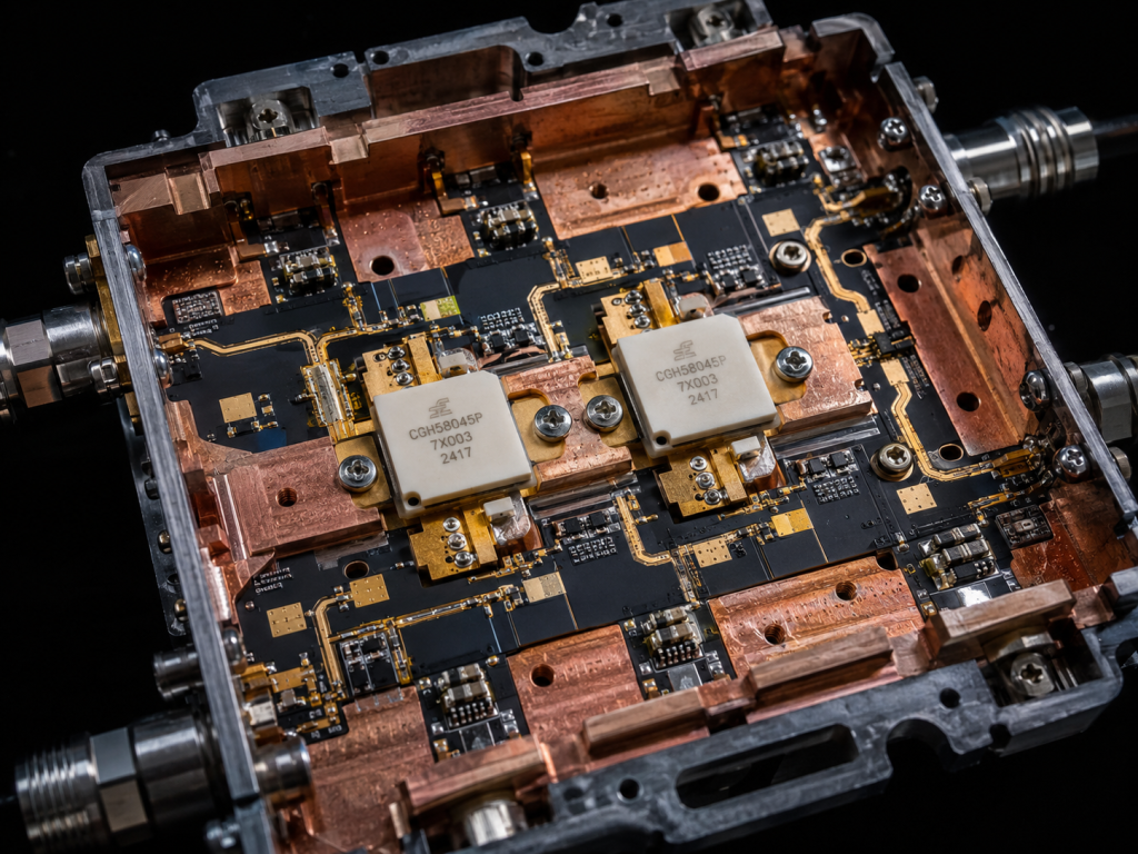
Stacking multiple attenuation blocks introduces cumulative Voltage Standing Wave Ratio penalties into your network. Each mismatched junction generates a separate reflection coefficient altering your primary forward wave. When testing radar antennas you need absolute certainty regarding incident power levels. A cascaded uncalibrated attenuator chain might present a combined 3:1 VSWR at 10 GHz. This physical mismatch physically alters any complex load impedance seen by your driving source. Your precision VNA receiver cannot differentiate between actual antenna roll-off and cable assembly losses. Consequently you record invalid gain flatness metrics masking true system capabilities. What’s a real story? microwave metrology demands strict calibration planes established via rigorous methodology. Inserting unknown passive elements ruins any previously established error correction models immediately. We must eliminate these cascaded variables achieving true engineering truth during critical evaluations. Relying on mathematical software compensation cannot fix a fundamentally broken hardware signal path. Professional integrators require solid transmission line architectures minimizing random phase shifts entirely. Utilizing a dedicated high-power amplifier ensures stable power delivery avoiding unpredictable attenuation artifacts. Another case study involves an electronic warfare team losing three weeks chasing phantom resonant frequencies.
3. Why Does Gain Flatness Distortion Wreck VNA Sweeps?
Analyzing Spectrum Anomalies
● Sweep Trace Ripples
● Parasitic Filter Effects
● Measurement Ambiguities
A typical vector network analyzer relies on precise port matching calculating S-parameters accurately. Gain flatness distortion manifests as a ripple effect spreading across your entire sweep trace. You require a stable baseline evaluating advanced electronic warfare active phased arrays. Any fluctuation exceeding ±3.5dB renders your specific frequency hopping algorithms completely untestable. Cascading uncalibrated attenuators creates resonant cavities acting like unintended narrow-band filters. These parasitic filter effects chew notches into your carefully planned link budget. An engineer reviewing this distorted data might incorrectly redesign a perfectly functional radiating element. Ready for a shock? hidden root causes remain inside an equipment rack. Replacing those unreliable external pads with a precisely matched amplifier solves this issue. We provide hardware delivering consistent wideband performance without relying on external hacking. A distorted VNA screen often prompts unnecessary hardware revisions wasting valuable engineering resources. Building an integrated RF front-end architecture provides a reliable foundation resolving these measurement ambiguities. You eliminate unpredictable resonant frequencies by utilizing factory-calibrated active amplification modules directly. A third example demonstrates how implementing proper active amplification restored VNA calibration baseline integrity immediately.
S-Parameter Distortion | Symptom | VNA Display Result
Mismatched Connectors | Reflection Spikes | High S11 Magnitude
Cascaded Attenuator Chain | Cumulative Phase Error | Wavy S21 Gain Response
Cable Flexing | Phase Instability | Fluctuating Transmission Phase
4. What Defines Effective RF Front-End Architecture Link Budgeting?
Upstream System Thinking
● Insertion Loss Calculations
● Drive Strength Guarantees
● Amplitude Stability
Designing a robust test architecture requires calculating every single decibel of loss meticulously. You cannot arbitrarily insert lossy components while expecting pristine signal integrity at an antenna feed horn. An optimal link budget accounts for specific insertion losses across all interconnecting RF cables. We must guarantee sufficient drive strength reaching your device under test during OTA evaluation. A solid hardware selection process prioritizes active modules with built-in gain flatness compensation. Utilizing CorelixRF design philosophy guarantees your signal chain maintains strict amplitude stability. We engineer our power amplifiers absorbing minor load variations without oscillating. But here’s a catch: most off-the-shelf amplifiers lack this necessary internal matching network. They require external isolators which only add more uncalibrated variables into your setup. Proper architecture design dictates integrating high-performance active blocks directly minimizing external passive clutter. A correctly calculated link budget guarantees your receiver captures accurate low-level return signals constantly. Relying on robust active components simplifies your overall system layout improving long-term measurement repeatability. Implementing a verified 52dB gain block eliminates any requirement regarding makeshift downstream signal boosting.
5. How Does VSWR Impact High-Frequency Pulse Delivery?
Addressing Reflected Energy
● Thermal Heat Generation
● Duty Cycle Stress
● Catastrophic Failure Prevention
Transmitting pulsed waveforms into a poorly matched antenna system generates immediate physical consequences. High VSWR conditions force massive amounts of localized energy back into your final transistor stages. This reflected power converts directly into destructive thermal heat within your sensitive gallium nitride devices. During a 50us pulse width transmission any instantaneous thermal gradient rises dramatically. A cascaded uncalibrated attenuator severely worsens this condition via unpredictable impedance transformations. A radar testing protocol demanding a 10% duty cycle heavily stresses standard cooling mechanisms. Without proper hardware matching logic any output power drops drastically from its 100W rated specification. Now consider this: continuous operation under high VSWR eventually leads toward catastrophic device failure. You need equipment capable of surviving a 2:1 mismatch without shutting down unexpectedly. We integrate specialized isolators internally protecting our circuitry from these harsh realities. An unprotected generic amplifier will quickly degrade providing inconsistent output levels during long test campaigns. Utilizing durable hardware guarantees your laboratory sustains continuous operational capability avoiding costly downtime.
Pulse Parameters | Value | Operational Impact
Pulse Width | 0.5 – 50 us | Determines Thermal Soak Time Duty Cycle | 0 – 10 % | Dictates Average Power Dissipation Input VSWR Limit | 2:1 | Defines Maximum Safe Reflection
6. Why Bring CorelixRF Engineering Truth To OTA Testing?
Eradicating Laboratory Guesswork
● Verifiable Measured Data
● B2B System Integration
● Repeatable Metrics
We reject an industry trend of providing generic marketing specifications masking poor component performance. Engineering truth means delivering actual measured data reflecting real-world microwave environments accurately. We test our modules extensively under mismatched conditions mimicking your exact antenna chamber setup. Our factory focuses exclusively on providing reliable B2B solutions for demanding system integrators. You deserve components that perform exactly as documented on their official data sheets. CorelixRF builds hardware designed specifically for challenging radar and aviation control applications. What is a real deal? We manufacture specialized equipment solving complex RF front-end construction problems directly. There are no magical software fixes for fundamentally flawed physical transmission line layouts. We provide solid RF power solutions eliminating any need for cascaded uncalibrated attenuators entirely. Our approach guarantees repeatable gain flatness metrics across your entire testing campaign. We believe transparency regarding actual hardware limitations builds lasting trust alongside our global clientele. You receive accurate performance charts demonstrating true capabilities under rigorous pulsed operational scenarios.
7. How Does CRF-PA-8000M12000M-100W Circuit Integration Work?
Precision Hardware Deployment
● Frequency Range Capability
● Digital Interface Control
● Physical Port Integration
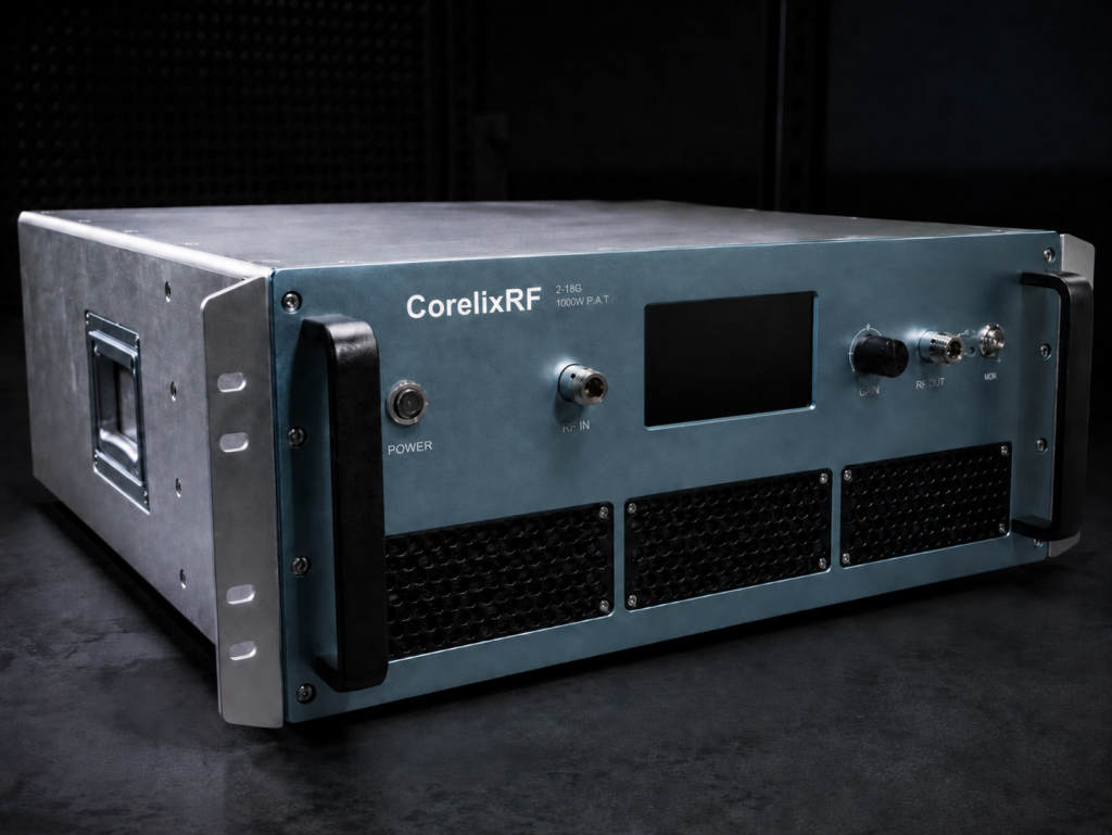
A CRF-PA-8000M12000M-100W module represents a structural paradigm shift in microwave power amplification. This unit operates seamlessly across an 8,000 through 12,000 MHz frequency range. It delivers a nominal gain of 52dB with a remarkably stable ±3.5dB flatness specification. We utilize a CAN interface enabling precise digital control during automated laboratory sequences. A physical package measures exactly 255 x 245 x 80 mm accommodating robust internal structures. Input signals enter through a standard SMA-Female connector providing reliable low-power connections. Amplified RF energy exits via a rugged N-Female port minimizing high-power insertion losses. Ready for a good part? This specific model outputs 100W of pulsed power consistently. We eliminate measurement ambiguities by integrating precise matching networks directly within a primary chassis. Integrating this specific module standardizes your testing rack eliminating messy custom coaxial assemblies. A streamlined hardware footprint provides your engineering team extra space accommodating additional diagnostic instrumentation. Providing robust connections drastically reduces intermittent contact issues plaguing legacy measurement setups.
Specifications | Minimum | Typical | Maximum
Frequency Range (MHz) | 8,000 | – | 12,000 Gain (dB) | 52 | – | – Gain Flatness (dB) | -3.5 | – | 3.5
8. What Drives High-Frequency Material Selection And Thermal Dissipation?
Managing GaN Temperatures
● Dielectric Loss Tangents
● Heatsink Requirements
● Impedance Matching
Constructing a broadband 100W amplifier requires utilizing advanced Gallium Nitride semiconductor technology exclusively. GaN transistors provide superior power density but generate intense localized heat spots rapidly. We mandate a massive heatsink attachment maintaining an operating temperature between 0 and 50 C. Proper thermal dissipation prevents gain compression anomalies during extended antenna evaluation procedures. We select high-frequency PCB laminates exhibiting extremely low dielectric loss tangents. These premium materials guarantee your signal phase remains coherent traversing an amplifier circuit. Using cheap substrates would reintroduce distortion variables we are attempting currently resolving. Think about this: poor thermal management physically alters electrical characteristics of any RF device. Our rigorous material selection guarantees constant 50 ohm impedance matching across all operating conditions. We engineer an internal layout maximizing heat transfer away from sensitive active junctions. This dedication regarding superior thermal engineering guarantees consistent output power during prolonged testing intervals. A stable thermal profile translates directly into highly repeatable S-parameter measurements verifying your antenna design.
9. How Do Advanced Built-in Protection Mechanisms Handle Mismatch?
Safeguarding Expensive Test Assets
● Over-Voltage Defenses
● Current Limiting Protocols
● Active VSWR Monitoring
Operating inside an experimental OTA chamber exposes hardware toward unpredictable physical connection failures. An accidental cable disconnect instantly presents an infinite VSWR toward your transmitting source. Our CRF-PA-8000M12000M-100W incorporates sophisticated built-in protection circuits monitoring critical node voltages constantly. A system detects over-voltage conditions and shuts down a DC 28V supply immediately. We also implement rapid over-current limiting preventing catastrophic transistor cascade failures. Specialized over-temperature sensors throttle performance if an external heatsink becomes compromised during operation. Here is an exciting detail: our active VSWR protection circuitry dynamically monitors reverse power levels. It reacts within microseconds preventing severe damage from improperly mated N-Female connectors. You can conduct interference testing with complete confidence in your primary hardware. CorelixRF builds equipment designed surviving a harsh reality of daily engineering laboratory use. These advanced protective measures vastly extend an operational lifespan defining true return on investment. Your procurement department appreciates hardware functioning reliably eliminating constant repair cycle budgetary drains.
Protection Mechanisms | Trigger Condition | System Response
Over-Voltage | Supply Fault | Immediate DC Cutoff Over-Temperature | High Thermal Load | Power Throttle VSWR Mismatch | Reflection > 2:1 | Fast RF Blanking
10. How Should System Integrators Deploy Reliable RF Front-Ends?
Optimizing Laboratory Infrastructure
● Calibrated Amplification Modules
● Harmonic Suppression
● Spurious Emissions Control
Radar developers must prioritize acquiring calibrated amplification modules featuring integrated protection systems. Relying on cascaded uncalibrated attenuators guarantees compromised test data and wasted engineering hours. Deploying a CRF-PA-8000M12000M-100W standardizes your test bench providing a verified stable reference plane. You achieve superior harmonic suppression rated at -20 dBc improving overall signal purity. A unit maintains spurious emissions at a remarkably low -60 dBc securing regulatory compliance. We provide detailed mechanical drawings assisting your mechanical team with rack installation planning. It boils down here: professional testing requires professional-grade signal generation and amplification. Stop troubleshooting test equipment and start characterizing advanced antenna arrays effectively. Utilizing our hardware matching logic eliminates variables distorting critical gain flatness measurements. Partner with CorelixRF securing dependable microwave power solutions grounded in verifiable engineering reality. We stand ready assisting your system integrators achieving flawless RF front-end architectures immediately. Your next generation radar platform requires a stable testing foundation guaranteeing accurate field deployment performance.
Wrapping up our analysis constructing a reliable antenna OTA testing environment demands precise hardware matching logic. Eliminating cascaded uncalibrated attenuators prevents severe gain flatness test data distortion entirely. You must integrate robust active modules like a CRF-PA-8000M12000M-100W into your architecture. Stop compromising laboratory results utilizing inadequate passive components during critical evaluation phases. Contact CorelixRF today securing a specialized data sheet for your next integration project. We provide proven microwave solutions solving complex electronic warfare laboratory challenges.
- Q1: What is Antenna OTA RF Front-End Construction?
- Antenna OTA RF front-end construction involves assembling amplifiers bypassing unstable cables transmitting signals effectively.
- Q2: How does a CRF-PA-8000M12000M-100W work?
- It amplifies 8,000 through 12,000 MHz signals up toward 100W utilizing reliable GaN technology.
- Q3: Why do uncalibrated attenuators distort test data?
- They introduce cumulative impedance mismatches causing unpredictable gain flatness ripples across broadband frequency sweeps.
- Q4: What causes VSWR spikes during chamber testing?
- Poorly mated connectors alongside aging absorbing cones reflect transmitted energy backwards toward a source.
- Q5: How do you eliminate gain flatness distortion?
- Deploying a precisely matched power amplifier removes any need regarding unpredictable cascaded passive pads.
Turn VSWR behavior into factory acceptance evidence
High VSWR protection should be defined with mismatch scenario, foldback or shutdown threshold, recovery logic, alarm output, thermal limit and FAT evidence. This makes protection claims measurable for procurement.
Recommended next step: send the operating band, output power target, duty cycle, load condition, control interface, protection or thermal limits and required FAT documents. CorelixRF can review this How to Protect Antenna OTA RF Front-End Architectures from VSWR Spikes? requirement against standard RF amplifier platforms, RF front-end options and controlled customization paths.