
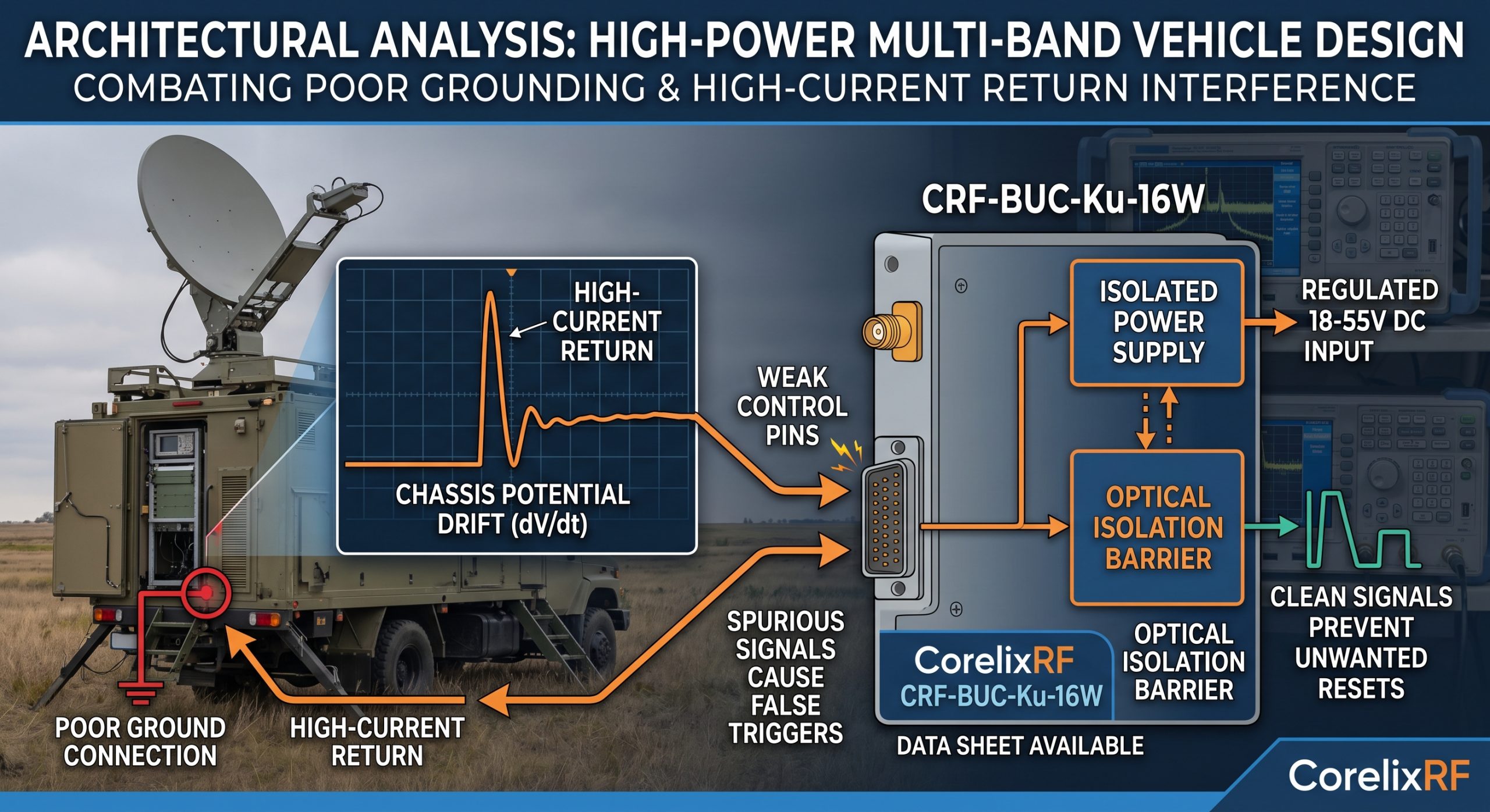
System engineers face brutal realities daily. A mobile VSAT platform transmits a burst. Command screens flash a sudden VSWR fault. Output power vanishes instantly. Here is the deal. That failure rarely stems from damaged antennas. Instead, high-current return paths shift chassis potential. This voltage transient injects noise into weak RS485 logic pins. We manufacture industrial microwave hardware, meaning we analyze these specific failures deeply. Proper system architecture demands rigid isolation techniques alongside robust components.
1. The Reality of Vehicle Grounding Failures
Mobile communication arrays operate inside harsh electrical boundaries. High-frequency vibration loosens mechanical joints constantly. A standard 80W load operating at 24V draws substantial current. This current must find a path back toward its source. What represents our real story? Steel vehicle frames offer unpredictable electrical resistance. An engineer measuring continuity with a multimeter sees zero ohms. However, dynamic RF bursts present entirely different impedance characteristics. Fast transient currents encounter parasitic inductance across those metal joints. This creates localized voltage gradients along equipment racks. An IP65 rated enclosure might sit at one potential. Central control units sit at another potential entirely. When a transmit command executes, that potential difference spikes. Weak current control lines absorb this differential voltage directly. Your RS485 transceiver misinterprets this noise as a reset command. Entire transmission sequences abort prematurely. We observe this specific phenomenon repeatedly during field troubleshooting sessions. Operators often blame thermal shutdown or component degradation incorrectly. You must address current return paths systematically.
Transient Voltage Generation Across Chassis Joints
| Parameter | Current Burst Peak | Joint Inductance | Resulting Voltage Shift |
| Clean Bonding | 3.0 A | 10 nH | 30 mV |
| Mild Oxidation | 3.0 A | 100 nH | 300 mV |
| Severe Degradation | 3.0 A | 500 nH | 1.5 V |
| Critical Failure | 5.0 A | 1000 nH | 5.0 V |
2. Mechanism of High-Current Return Interference
Understanding transient interference requires analyzing basic electrical physics. Ohm’s law remains absolute within microwave engineering domains. High-efficiency GaN amplifiers switch with extreme speed. These rapid transitions generate massive dI/dt events during operation. This is where things get interesting. Such rapid current changes interact violently with stray inductance. A perfectly shielded RF cable still contains outer conductor resistance. When chassis ground degrades, DC return current seeks alternate routes. It flows backward through braided coaxial shields. Baseband noise directly couples into sensitive internal circuitry. This mechanism degrades your local oscillator phase noise significantly. A specification sheet might promise -73 dBc/Hz at 1 kHz offset. Real-world performance collapses under heavy ground loop conditions. Resulting jitter ruins complex modulation schemes immediately. Engineers attempting field diagnostics usually look at spectrum analyzers. They notice elevated noise floors extending across wide bandwidths. They rarely suspect a rusted bolt holding a grounding strap. System architecture must anticipate and block these rogue current paths.
Phase Noise Degradation versus Ground Loop Current
| Return Current on Shield | 100 Hz Offset | 1 kHz Offset | 10 kHz Offset |
| 0 mA (Isolated) | -63 dBc/Hz | -73 dBc/Hz | -83 dBc/Hz |
| 50 mA | -58 dBc/Hz | -68 dBc/Hz | -79 dBc/Hz |
| 200 mA | -45 dBc/Hz | -55 dBc/Hz | -70 dBc/Hz |
| 500 mA | Loss of Lock | Loss of Lock | Loss of Lock |
3. Architectural Design Flaws in Multi-Band Systems
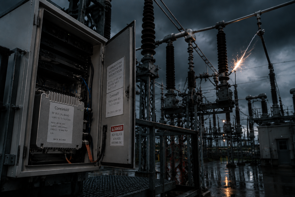
Commercial off-the-shelf components frequently introduce severe architectural vulnerabilities. Procurement teams often select hardware based purely upon price. They ignore critical internal grounding methodologies entirely. Let that sink in. Cheap power amplifiers tie DC negative directly against RF signal ground. This creates a permanent unresolvable loop within any mobile installation. Multi-band vehicles integrate multiple high-power transceivers near each other. Each unit injects broadband noise back into shared power buses. An engineer fighting these issues often deploys massive ferrite beads. Ferrites only mask symptoms rather than curing root causes. Upstream system thinking dictates completely isolated power supply designs. You need floating DC inputs capable of rejecting massive common-mode transients. A weak logic pin lacking optical isolation will eventually fail. That resulting false trigger disables mission-critical radar or communications gear. We analyze these failed commercial boards inside our laboratory frequently. We find blown RS485 chips surrounded by perfectly intact RF transistors. System integrators must evaluate internal circuit topologies during BOM selection.
Comparative Analysis of Internal Isolation Topologies
| Topology Type | DC Return Path | Logic Interface | Susceptibility to Ground Bounce |
| Commercial Standard | Tied to chassis | Direct coupled | Extremely High |
| Quasi-Isolated | Capacitively coupled | Resistive pad | Moderate |
| CorelixRF Industrial | Fully floating DC | Optically isolated | Near Zero |
| Aerospace Grade | Galvanic isolation | Fiber optic | Zero |
4. Thermal Dissipation and Mechanical Grounding Synergy
Mechanical engineering directly influences high-frequency electromagnetic performance. Heat sinks do much more than simply remove thermal energy. They function as large continuous equipotential reference planes. But here lies a catch. A module measuring 145 x 80 x 70 mm requires careful mounting. Our one kilogram package relies upon flat surface contact. Poor machining on a mounting plate introduces microscopic air gaps. These gaps act as parasitic capacitors during high-frequency operation. Such capacitance severely disrupts continuous ground shielding effectiveness. RF currents pool around mounting bolts instead of distributing evenly. This uneven distribution radiates energy back into adjacent wiring harnesses. Thermal interface materials must also provide excellent electrical conductivity. Engineers sometimes apply thick non-conductive thermal paste generously. They solve their heat problem while simultaneously creating an RF nightmare. Proper architecture requires specifying conductive gaskets matching specific compression metrics. Air cooling paths must never compromise this crucial mechanical bonding layer. We provide comprehensive mechanical outlines precisely for this critical integration phase.
Thermal Interface Material Impact on RF Grounding
| Material Type | Thermal Conductivity | Volume Resistivity | High-Frequency Shielding |
| Standard Paste | 4.0 W/m-K | > 10^12 Ohm-cm | Poor |
| Ceramic Pad | 6.0 W/m-K | > 10^10 Ohm-cm | Poor |
| Silver Filled Elastomer | 3.5 W/m-K | 0.005 Ohm-cm | Excellent |
| CorelixRF Spec Gasket | 5.0 W/m-K | 0.002 Ohm-cm | Superior |
5. CorelixRF Solution: CRF-BUC-Ku-16W Hardware Isolation
Engineering truth demands rigorous hardware solutions over software patches. We developed the CRF-BUC-Ku-16W Block Upconverter specifically addressing these brutal realities. It outputs 42 dBm across a 13.75 to 14.5 GHz range. Here remains our bottom line. This unit fundamentally rejects chassis voltage transients through intelligent power design. We implemented an ultra-wide 18 to 55 V DC input range. This switching regulator design easily absorbs massive ground bounce events. A transient dropping your supply down suddenly will not trigger resets. Power and communication route exclusively through a PT02E-14-12 circular connector. We optically isolate every single RS485 and Ethernet control line internally. A three-volt chassis shift cannot physically reach our sensitive microprocessor pins. We maintain continuous ≥65 dB small signal gain unconditionally. Your control system maintains absolute authority over its 20 dB adjustment range. Our high-efficiency GaN architecture consumes merely 80W typical during full transmission. This specific combination of wide-input regulation and optical isolation eliminates false triggering.
CRF-BUC-Ku-16W Core Specifications and Protection Mechanisms
| Parameter | Specification | Engineering Benefit |
| Operating Frequency | 13.75 – 14.5 GHz | Covers standard Ku band entirely |
| Rated Output Power | 42 dBm (16 W) | High linear power delivery |
| Supply Voltage | 18 – 55 V DC | Immune to voltage sags |
| Interface Isolation | Optical on RS485 | Prevents false logic triggers |
6. Front-End Matching Under Voltage Stress
Microwave impedance matching degrades severely when internal bias voltages fluctuate. An unstable ground reference directly modulates GaN gate bias levels. You might ask yourself why. Altered bias states change transistor output impedance dynamically. This changing impedance battles against your fixed waveguide structure constantly. A WR75 output port expects a stable source impedance continuously. When transients hit, internal reflections bounce between matching stages violently. This interaction spawns massive intermodulation products quickly. We engineer our matching networks handling a 2:1 output VSWR effortlessly. Our circuits clamp bias voltages relative to localized source pins strictly. Chassis voltage shifts cannot alter that gate-to-source potential difference. Third-order intermodulation remains firmly ≤-25 dBc at 3 dB back-off. Spurious emissions stay buried well below regulatory -55 dBc thresholds. Competitor modules often oscillate wildly during identical vehicle voltage dips. Maintaining strict RF metrics demands absolute DC stability at every node.
7. System-Level Link Budget and Phase Noise Integrity
A compromised link budget renders any communication hardware useless. Satellite uplinks require spectacular phase noise characteristics for high-order modulation. Our specification guarantees ≤ -93 dBc/Hz at a 100 kHz offset. What ruins these numbers? Ground noise injection destroys these figures instantly in poorly designed systems. We implement a strictly regulated 10 MHz reference frequency architecture. This unit accepts 0 dBm ±5 via its IF port securely. This reference dictates LO frequencies like 12.8 or 13.05 GHz perfectly. High-current return paths on vehicle chassis generate immense low-frequency magnetic fields. These fields induce currents across poorly shielded reference cables. We utilize heavy internal mumetal shielding separating power supplies from oscillators. Transmit in-band noise remains ≤-76 dBm/Hz regardless of external electrical chaos. Receive in-band noise stays exceptionally low at ≤-150 dBm/Hz. System integrators building maritime or ground VSAT base stations depend upon this. You cannot establish reliable links when vehicle alternators modulate your carrier.
8. Strategy for High-Efficiency GaN Modules
Gallium Nitride technology offers incredible power density advantages. However, it presents unique challenges regarding power supply decoupling. Fast switching edges demand instantaneous current delivery locally. Here stands a major problem. You cannot drag this current across a long noisy chassis. Our engineers deploy massive capacitor banks immediately adjacent near active devices. This localized energy storage prevents high-frequency demands from exiting our IP65 enclosure. We keep that dI/dt loop area microscopically small. Consequently, RF energy does not radiate out through your power connector. We utilize strict N-F input and WR75 output configurations blocking leakage. Operating safely between -40 and 60 degrees Celsius requires stable internal environments. Heat stresses decoupling capacitors, thereby increasing their equivalent series resistance. We select extreme-temperature rated components ensuring lifetime parameter stability. This uncompromising approach guarantees your 16W output remains pristine over decades. Source factories understand these deep material science interactions completely.
9. Engineering Practices for Installation and Routing
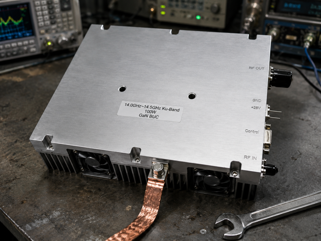
Superior hardware still requires correct physical installation methodologies. Engineers must stop treating mobile chassis metal as a zero-ohm conductor. This changes everything regarding integration. You must deploy dedicated heavy-gauge return cables directly from battery terminals. Never bond your DC negative against an equipment rack locally. RF grounding requires entirely separate wide braided straps. Connect these straps directly between our aluminum housing and true vehicle ground. Keep these RF bonds incredibly short minimizing parasitic inductance. Apply conductive anti-oxidant compounds across all mechanical mating surfaces carefully. Shielded twisted pairs must carry all RS485 communication signals. Ground this shield at one single point avoiding low-frequency loops. Monitor your 950 – 1450 MHz IF frequency range using isolated spectrum analyzers. Following these strict engineering guidelines extracts maximum performance from industrial modules. We supply pattern files and complete mechanical outlines assisting this critical integration.
10. Conclusion
Architecture Analysis: High-Power Multi-Band Vehicle Design Essentials – Combating Poor Grounding and High-Current Return Interference Causing False Triggering. System architecture ultimately dictates hardware survival inside mobile environments. Poor grounding creates massive voltage transients during high-current transmit bursts. These transients falsely trigger weak control pins and destroy link budgets. Our CRF-BUC-Ku-16W isolates these threats using wide-input regulation and optical barriers. Stop fighting erratic alarms using generic unprotected commercial modules. Contact CorelixRF engineering teams evaluating robust power amplifiers for your next integration.
FAQ Section
Q1: What is the most common cause of false triggering in mobile RF systems?
High-current return paths shifting chassis potential cause false triggering. This injects severe voltage transients directly into sensitive logic pins.
Q2: How does the CRF-BUC-Ku-16W handle extreme voltage fluctuations?
It employs a highly isolated 18 to 55 V DC input range. This prevents chassis ground bounce from affecting internal bias networks.
Q3: Why do standard commercial amplifiers fail in multi-band vehicle environments?
They tie DC return directly with RF signal ground internally. This allows high-power transient noise to corrupt local oscillator phase noise.
Q4: What role does the mechanical heat sink play in RF grounding?
The heat sink acts as a continuous equipotential reference plane. Poor machining creates parasitic capacitance which disrupts effective high-frequency shielding.
Q5: How should engineers route power cables for high-power vehicle RF modules?
Engineers must run dedicated return wires directly back from battery terminals. Never rely upon the steel vehicle chassis for DC current return.
Review vehicle VSAT grounding as a complete RF chain
High-current return interference is rarely solved by one component. Share the vehicle ground path, BUC/LNB chain, amplifier power margin, cable routing, shielding, signal source and environmental limits so engineering can review the full RF path.
Recommended next step: send the operating band, output power target, duty cycle, load condition, control interface, grounding or thermal limits and required FAT documents. CorelixRF can review this vehicle VSAT high-current return interference requirement against standard RF amplifier platforms, RF front-end options and controlled customization paths.